


A new paper recently published reports the integration of the GETec atomic force microscope (AFSEM) into a helium ion microscope (HIM). Combining the two techniques opens the way for unprecedented, in situ, correlative analysis at the nanoscale.
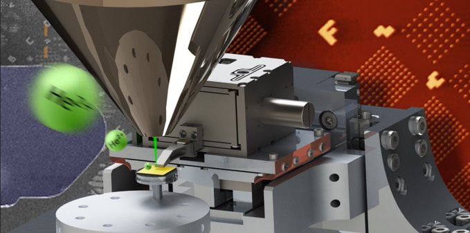
In this work, GETec report the integration of an atomic force microscope (AFM) into a helium ion microscope (HIM). The HIM is a powerful instrument, capable of sub-nanometer resolution imaging and machining of nanoscale structures, while the AFM is a well-established versatile tool for multiparametric nanoscale characterisation.
Combining the two techniques opens the way for unprecedented, in situ, correlative analysis at the nanoscale. Nanomachining and analysis can be performed without contamination of the sample and environmental changes between processing steps. The practicality of the resulting tool lies in the complementarity of the two techniques. The AFM offers not only true 3D topography maps, something the HIM can only provide in an indirect way but also allows for nanomechanical property mapping, as well as for electrical and magnetic characterisation of the sample after focused ion beam materials modification with the HIM. The experimental setup is described and evaluated through a series of correlative experiments, demonstrating the feasibility of the integration.
In situ AFM analysis in your SEM
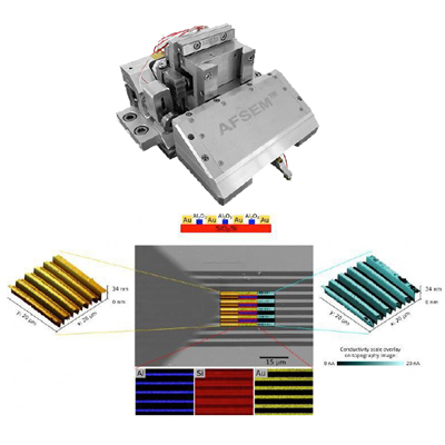
AFSEM is an atomic force microscope (AFM) by GETec Microscopy, designed for integration in a SEM or Dual beam (SEM/FIB) microscope. Its open access design allows to simultaneously operate SEM and AFM inside the SEM vacuum chamber. The complimentary image data of AFM and SEM enable unique characterisation of your sample.
AFSEM lets you simultaneously image your sample with high resolution, create true 3D-topography representations, and accurately measure heights, distances and even material properties, all while maintaining the large SEM field of view to position your AFSEM™ cantilever exactly where you want it.
AFSEM fits into most SEM or dual beam (SEM/FIB) systems: it is mounted directly on the door of the system chamber, leaving the stage unaltered. In addition, a slim tip-scanning design in combination with self-sensing cantilevers requires only 4.5 mm space between the pole shoe of the electron column and the sample. As a result, AFSEM is compatible with a wide range of standard and optional stages, and can handle virtually any sample that fits the system chamber. This elegant design allows detection of sub-nanometer step heights in the SEM.


