
- Features
- Models
- Specifications
- Downloads
- Applications
- Related Products
- Contact
- Back To Spectroscopy
- Back To Optics
- Back To Hyperspectral
- Back To Cameras
- Back To X-Ray
- Back To Light Measurement
- Back To Characterisation
- Back To Electron Microscopy
- Back To Magnetometry
- Back To Ellipsometers
- Back To Cryogenics
- Back To Lake Shore
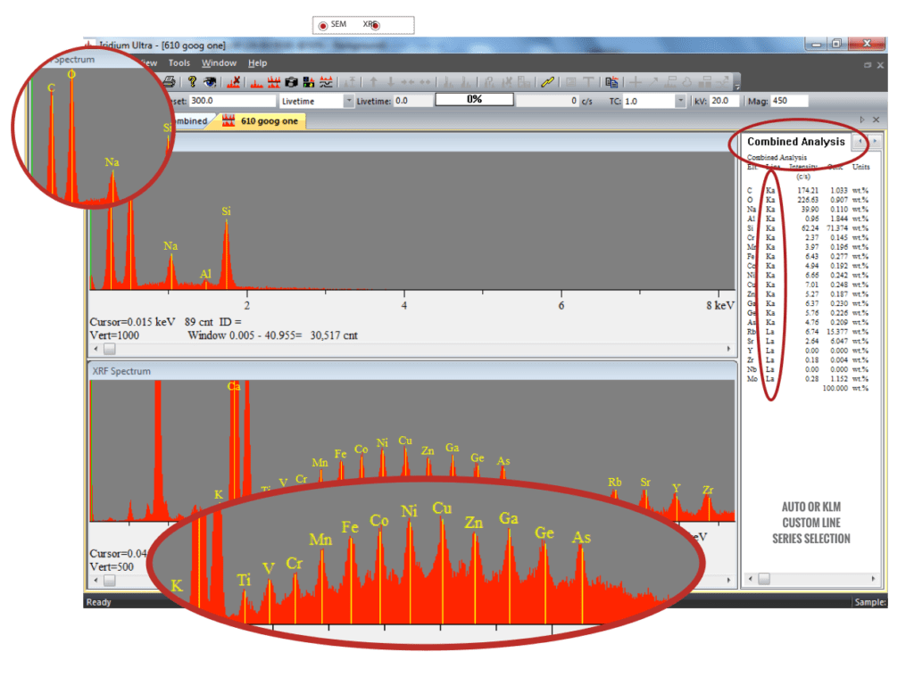
IXRF SEM/XRF
X-ray Sources for Electron Microscopy (SEM)
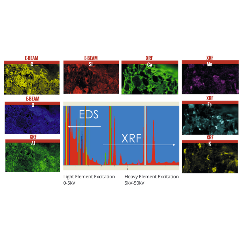
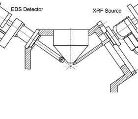
IXRF Systems’ microXRF X-ray sources for Scanning Electron Microscopes (SEM): addition of an polycapillary X-ray tube and Iridium Ultra software will transform your SEM’s quantitative analytical capabilities. Higher peak to background ratios enable greater elemental sensitivity for higher Z elements: sensitivity exceeding e–-beam excitation by a factor of 10-1000X. Exceptional beam stability, together with a modern SDD X-ray detector, afford higher precision with ppm-level sensitivity. Non-conductive materials may be analysed without any special preparation or coating. IXRF integrates with your SEM to deliver full spectrum analysis using excitation from both the e–-beam and X-ray source.
IXRF’s Xb SEM micro-spot X-ray source adds the capabilities of a complete micro X-ray fluorescence (microXRF) spectrometer to a scanning electron microscope (SEM). Xb SEM fits on an unused or open high-angle port of almost any SEM. Total non-destructive, μXRF users benefit from both superior trace element sensitivity and broader elemental coverage (Na through U using K- and L-lines).
Elemental Analysis with a microXRF Spectrometer
- Analytical results compare to those of standalone μXRF systems
- State-of-the-art analytical software: Iridium Ultra
- Decades of continuous development & innovation
- Selectable primary X-ray filters
- To suppress Bremßtrahlung and diffraction peaks
- For lower detection limits, down to PPM levels for most elements
- Uses your scanning electron microscope’s motorised stage
- Allows sample tilt to produce minimum spot sizes
- No special cooling is required, our sources are air cooled
Profile

Profile
Profile

Profile

Profile

Profile

Profile

CAPABILITIES
Xb Product Features
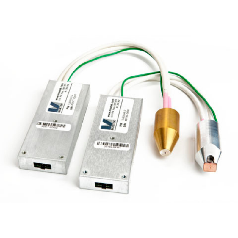
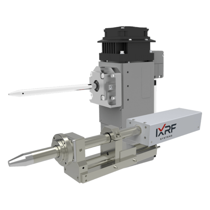
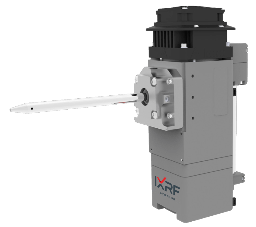
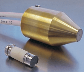
IXRF’s Xb custom micro-spot X-ray source is designed exclusively for use on electron microscopes. A compact design with slide mounting allow very close coupling to the sample. Patented polycapillary optics focus X-ray photons down to sample spot size as small as 10µ. Xb is offered in 10µm and 40µm spot sizes. An integrated high-voltage power supply operates up to a maximum power of 50 watts (35-50 kV and 1.0 mA depending on anode material). Close coupling provides XRF analytical results comparable to those from traditional “’benchtop EDXRF” or “mainframe” XRF instruments. An additional benefit is that the Xb X-ray source is designed so that it does not interfere with the normal operation of the electron microscope, including the use of the electron beam on the same sample at the same time so as to simultaneously collect data on all elements.
SEM-XRF Advantage: Quantify Trace Elements
Electron beams (from scanning electron microscopes) produce very high backgrounds, hiding trace elements in a sample. Direct X-ray excitation from a true “X-ray source” don’t have this effect. Using IXRF’s Xb, low ppm levels of elements can be easily identified, quantified … even producing trace level X-ray maps to view elemental distribution of trace elements in your sample. For elements above Na, limits of detection (LOD) can be as low as 10 ppm, depending on element and matrix.
SEM-XRF Advantage: Broad Elemental Coverage
X-ray excitation up to 50 kV, together with a variety of available primary filters, allows for high-sensitivity analysis of first and second row transition metals (using K-lines). Even heavier elements may be similarly analysed using their L-lines.
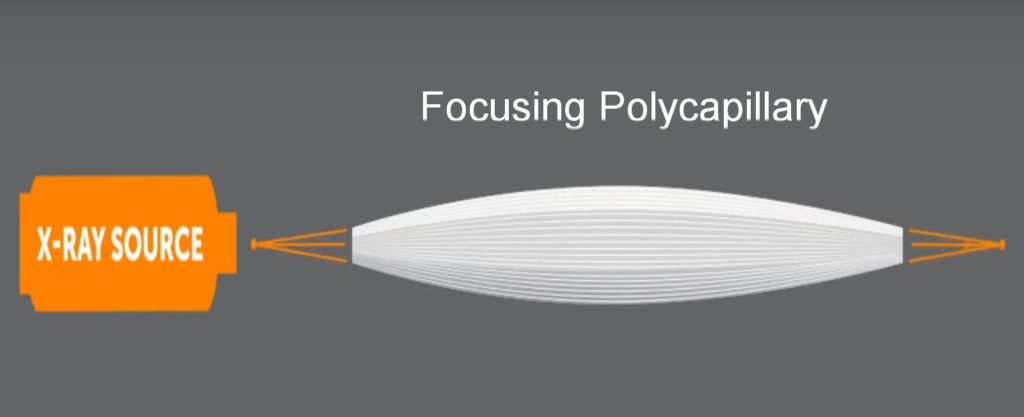
Polycapillary Optics’ Advantage
Polycapillary focusing optics collect a large solid angle of X-rays from an X-ray source and focus them to a spot as small as 10 µm. The X-ray flux density obtained is a few orders of magnitude higher than that obtained with a conventional pinhole collimator. The main application of these optics is micro X-ray fluorescence (µXRF) analysis, which has been widely used for thin film and plating analysis, precious metal evaluation, alloy measurement, and monitoring of electric circuit board coatings. Use of polycapillary focusing optics will significantly enhance the detection sensitivity and allow the high performance to be achieved with low-powered X-ray tubes. Micron-sized spatial resolution makes small feature evaluation possible for electronics and precious metal applications. Polycapillary optics offer 100x-10,000x gain with output focal spot sizes as small as 10 µm.
ƒX Product Features
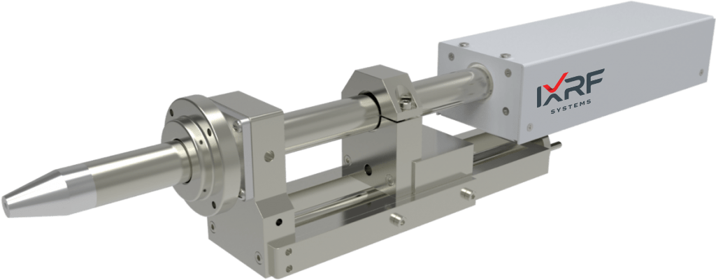
IXRF’s new ƒX SEM™ is an affordable, air-cooled custom X-ray source option designed exclusively for use on electron microscopes. With a compact design and slide mounting, very close coupling to the sample is achieved. This unique design delivers “high flux” X-rays to small or large excitation areas on a sample’s surface. The ƒX SEM™ offers excitation spots ranging from 500 µm to 25 mm (ellipse minor side width).
Supported On All SEM Brands
The integrated high-voltage power supply operates up to a maximum power of 10 W (35 kV and 0.1 mA depending on anode material). Close coupling provides X-ray fluorescence (XRF) spectrometry analytical results comparable to those from a traditional benchtop EDXRF operating under a vacuum atmosphere. The ƒX SEM™ is designed so that it does not interfere with the normal operation of the electron microscope, including the use of the electron beam on the same sample, at the same time collecting all elements simultaneously.
Non-destructively Quantify and Map Trace Elements
Electron beams (from scanning electron microscopes) produce very high backgrounds hiding the trace elements in the sample. X-rays, from a true “X-ray source” don’t have this effect. Using the ƒX SEM™ low ppm levels of elements can be easily identified and quantified … even producing trace level X-ray maps to view elemental distribution of trace elements in your sample.
X-ray Source + SEM =
- Sensitivity: Higher peak to background ratios enables greater elemental sensitivity for higher Z elements; sensitivity exceeding SEM/EDS by a factor of 10-1000x.
- Precision: The extreme X-ray beam stability of Xb, coupled with premium SDD X-ray detectors, yields highest possible precision and lowest achievable detection limits.
- Accuracy: Using elemental K-lines (and L-lines of high-Z elements) means less complex deconvolution of various peak overlaps.
- Non-destructive: Analysis of non-conductive materials without coating or e⁻-beam damage.
- Full elemental coverage: Integrated with EDS software for the most accurate low energy-high energy (full spectrum) analysis available (by combining e⁻-beam and X-ray beam excitation).
Fits Your Microscope
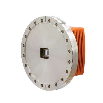
X-ray tube additions may be interfaced to almost any brand and model of SEM. High angle (35º) as well as horizontal flange mounts are available for every tube package.
Polycapillary Optics
IXRF’s Xb delivers the addition of focusing capillary optics to enable microspot XRF analysis down to 10 microns. A greatly reduced spot size increases micro-XRF X-ray elemental mapping capabilities and enhances trace elemental and/or thin-film analysis at the micron level.
10 μm Spatial Resolution
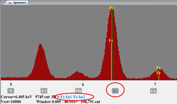
This is a picture of a 12 micron Ni grid X-ray map. The grid is imaged with a 10 micron Xb X-ray source demonstrating exceptional spatial resolution.
Combined EDS and XRF X-ray mapping bring previously unseen capability to the electron microscopist.

X-ray Tube Automation
Packaged tubes may be operated up to 50kV and come with integral high voltage power supplies. Power supplies are integrated with interlocking vacuum sensors which shut off the x-rays when the SEM chamber is vented. Each unit automatically “ramps” the tubes for increased longevity.
Miniaturisation
The chief component of low cost X-ray Fluorescence brought into the electron microscope chamber is the ƒX SEM™ low powered transmission target X-ray tube. The tubes are reduced in size and produce less heat than larger, higher powered tubes. Mo, W and Ag thin film targets deposited on a Be window are available for optimising varying applications.
X-ray source & Electron Beam Integrated Acquisition
- Multielement Quantitative Mapping
- Overlay Maps
- Map Analysis Suite (Toolbar)
- Extract Spectra (Freehand, Spot, Area)
- Extract Linescan
- DataView (Intensity/Concentration)
- Beam Drift Correction
- Maximum Pixel Spectrum
- Map stitch & montage
- Automate Stage and Beam automation
- Composition Mapping
- Phase Analysis
Available Methods
- Auto
- ZAF
- FP
- Least Squares
- Match
SPECIFICATIONS
- ANODE TYPE
- ACCELERATING VOLTAGE
0-50 kV
- BEAM CURRENT
Max 1 mA
- EXCITATION SPOT SIZE
10, 20, 40 µm
- COLLIMATOR SIZE
Patented polycapillary focusing optic
- SOURCE FILTERS
Available upon request
- COOLING REQUIREMENTS
Air cooled (fan)
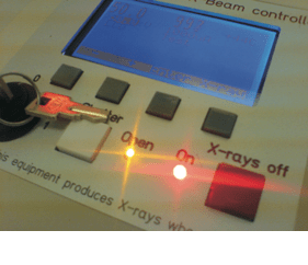
- CONTROLS / SAFETY
Variable control kV/µA, X-ray on/off buttons, kV/µA display, internal interlocked shutter. Interlocked to SEM, keyed power-on switch, HV-On lamp, warning beacon