
- Options
- Videos
- Downloads
- Applications
- Related Products
- Contact
- Back To Spectroscopy
- Back To Optics
- Back To Hyperspectral
- Back To Cameras
- Back To X-Ray
- Back To Light Measurement
- Back To Characterisation
- Back To Electron Microscopy
- Back To Magnetometry
- Back To Ellipsometers
- Back To Cryogenics
- Back To Lake Shore


NanoMEGAS Precession Electron Diffraction
Precession Enhanced Electron Diffraction application
The beam Precession in Transmission Electron Microscopes (TEMs) is a well-known technique to enhance dramatically the quality of the electron diffraction patterns, mitigating dynamical effect, increasing dps resolution, enhance bending and thickness effect, etc
Based on Precession Electron Diffraction (PED), NanoMEGAS offers since 2004 several automated and robust unique applications. A hardware (DigiSTAR P2010) to control specifically the coils of any TEM, is a scan and precession generator simultaneously, that is used either for static acquisition of ED, or scanning ED, suitable also for precession enhanced 4D-STEM (named 4D-SPED).
Additionally, NanoMEGAS offers acquisition platforms for static or scanning data collection,
together with dedicated software depending on the user application(s) preference.
Thus, full packages of the following applications is available:
- Orientation & Phase mapping
- Strain Mapping
- Precession enhanced 3D-ED for crystal structure determination
- Electron Pair Distribution Function (ePDF) for amorphous materials characterisation
- Electron Pair Distribution Function (ePDF) mapping
- Electric Field mapping
- Enhanced EELS and EDX Spectroscopy
Profile

Profile
Profile

Profile

Profile

Profile

Profile

OPTIONS
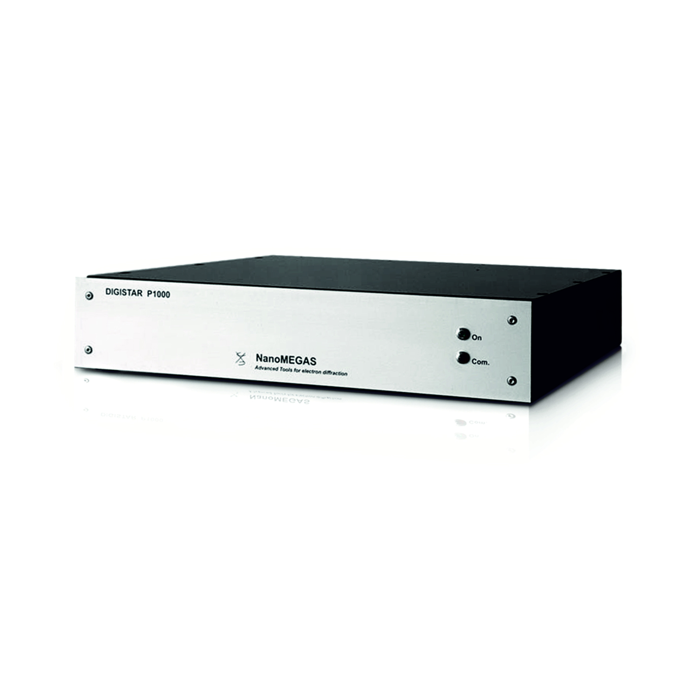
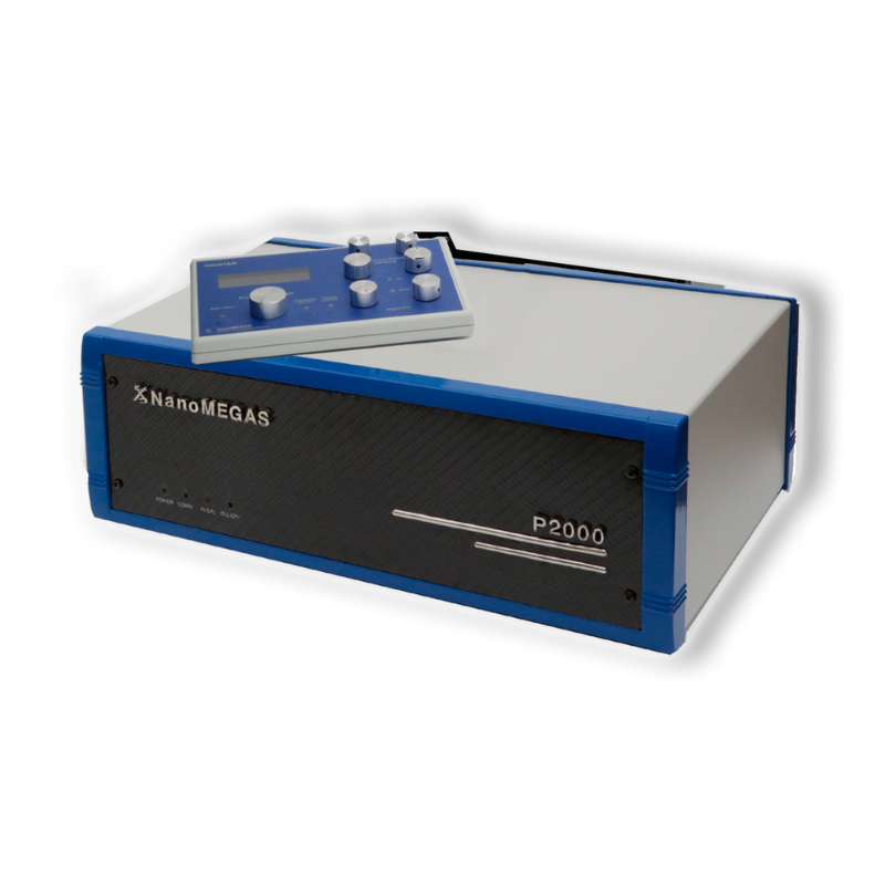
DigiSTAR P2010: Scan and Precession generator
The first commercially available precession and scan control globally, available for several applications and ideal for precession enhanced 4D-STEM application, as several detectors can be triggered, and data can be automatically saved in a ready-to-analysed format.
P2010 has been completely redesigned from 1st principles resulting in low distortion lower emissions product with full NRTL certification. Additional external synchronisation outputs have been added for hardware synchronising with on column accessories such as cameras and detectors. The standard installation now supports a distance of 10 m from the column with extension options available for remote installations up to 30 m. The new Digistar comes complete with 14 core IE9 processors and 32 GB of RAM with options of upgrading to 128 GB of RAM.

DigiSTAR P2010-Features
- Compatible with any TEM 120-200-300 Kv (LaB6 /W- FEG)
- Galvanic Isolation system (GIS) via optical fibre for TEM connection
- Retrofit between multiple TEMs in same lab
- High precession frequency >1kHz (depending on TEM)
- High Scanning speed >20kHz(depending on TEM)
- Precession semi-angle variable from 0- 85 mrad(TEM dependent), spot distortion correction-compensation at high angles ( > 15 mrad
- Simultaneous Scanning and Precession control
- Compatible with several high-end detectors (please ask)
- Dedicated straightforward automated software to control experimental settings
- Suitable for 4D-STEM and 4D-SPED acquisition
ASTAR: Orientation and Phase mapping
Automated orientation and phase mapping analysis of a variety of materials (metals, semiconductors, oxides etc.) by TEM using 4D-SPED technique consists of a successful application based on PED, called ASTAR. The major benefit of the technique is the high spatial resolution that can be down to 1-3 nm resolution (in case of FEG-TEM). Beam Precession is essential to improve data quality, in terms of dynamical effect reduction, and diffraction patterns increased resolution improving significantly the results reliability due to the present of higher order reflection. This application allows the user to further analyse their samples in nm scale, by Virtual Dark Field images, Texture analysis, Grain boundaries, Grain size distribution, etc

ASTAR-Features
- Orientation and Phase mapping of several kind of materials (alloys, metals, nanoparticles, nanowires, semiconductors, ceramics, batteries, etc)1
- Orientation (and phase) color maps that each color correspond to certain accurate crystal orientation (and phase) according to the crystal inverse pole figure colour map.
- Spatial resolution down to 1-2nm (TEM & sample depending)
- Precession: Mitigates dynamical effect (disappears possible Kikuchi lines) and enhance the reliability of the orientation and phase map, as higher order reflections are recorded.
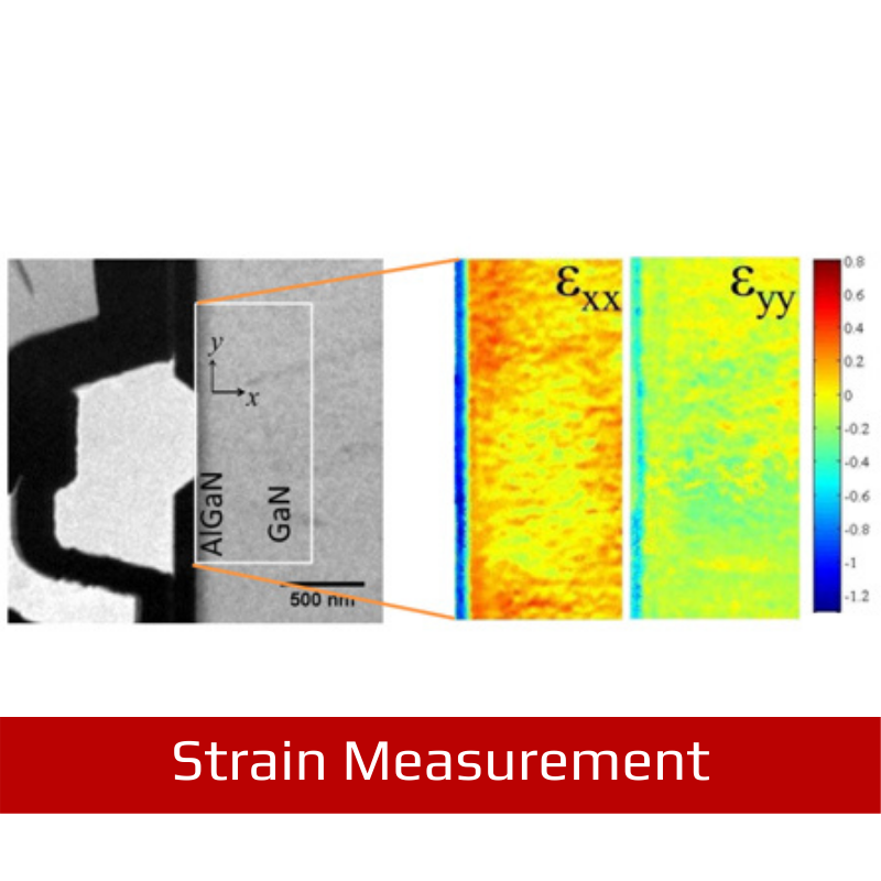
TopSPIN strain: Strain and Deformation analysis
The 4D-SPED acquisition method can also be applied to obtain strain mapping analysis (TopSPIN strain) of semiconductor materials at 1-4 nm resolution (sensitivity 0.02%), based on comparison of PED- patterns of strained areas with a reference (non-strained) area. The use of a precessing beam is essential for observing diffraction spots further away from the central spot, enhancing the strain sensitivity detection, and furthermore, improving any sample bending or thickness effect. Strain mapping analysis in TEM by 4D-SPED technique is a straightforward method that can be applied at any TEM and provides rapid and accurate data (same order of magnitude as dark field holography) without any requirement to index diffraction patterns, is critical to monitor the designed and unintended strain distributions.

TopSPIN strain-Features
- Strain analysis software for semiconductor materials and single crystal uniformly oriented systems.
- Strain sensitivity down to 0.1-0.01%
- Spatial resolution down to 1-5nm (TEM & sample depending)
- Precession: Facilitates the zone axis orientation of the sample, reduces the sensitivity of the sample thickness and bending effect, increase the number of higher order reflections, reduces dynamical scattering.

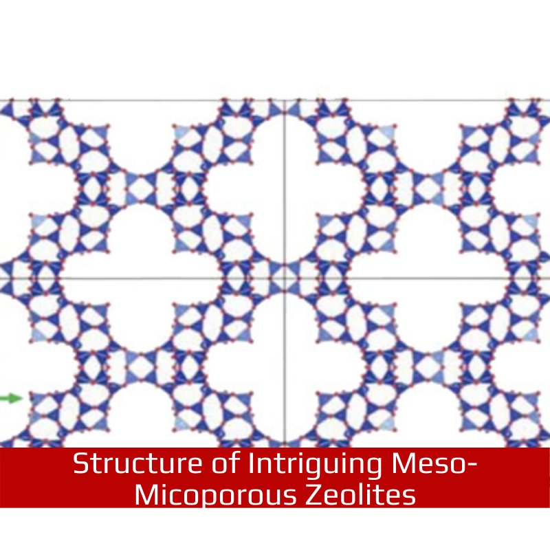
ADT-3D: PED tomography (Precession 3D-ED)
PED was firstly applied in electron crystallography, which in combination with 3D diffraction tomography (or 3D-ED, MicroED) in TEM, has become a critical method for structure determination of various nanocrystals, from minerals and alloys to complex zeolites, MOFs, organic compounds and proteins. In the conventional PED tomography method, a series of ED patterns are collected in a TEM every 1degree of tilting around the goniometer axis. Acquired data are automatically processed by specific software (ADT-3D). Specifically, the diffraction patterns are merged towards the reciprocal space 3D reconstruction, cell parameters determination, indexing and intensities measurement used for ab initio crystal structure determination .

ADT-3D-Features
- Ab-initio structure determination of (any nanostructure) metals, ceramics, polymers, semiconductors, pharmaceuticals, organics, proteins etc
- Cell parameters determination
- Symmetry determination for nanocrystals (space and point group)
- Merging several ED data sets
- Reflections integrations by Precession
- Increased resolution in ED patterns through Precession
- Analysis of twin crystal datasets
- Diffuse scattering for further disorder modelling
ePDF basic: Amorphous Materials Characterisation
Precession electron diffraction in TEM is reported to provide high quality data for analysis of amorphous or nanocrystalline materials. Typical total scattering patterns are acquired in TEM in a few seconds, a speed only matched by synchrotron radiation (lab X-ray acquisition is a much more time-consuming approach for such materials (2-20 hours). The total scattering data are processed by a specific software (ePDF) using the well-known Pair Distribution Function method. Amorphous and/or nanocrystalline materials can not only be identified but furthermore can be characterised through the interatomic distances from the PDF diagram.

ePDF basic-Features
- ePDF calculation using PED data
- Interatomic distances identification
- Simulations of ePDF from know crystal structures
- Pearson Correlation
- Pattern summation (new feature)
- Automatic beam stopper determination
- Automated diffraction centre determination and position adjustment
- Automatic calculation of peak positions for any calculated ePDF from experimental data
- Overlay of bond distances or simulated PDFs calculated using any CIF file on the experimental ePDF
- Normalisation of ePDF during overlay
ePDF advanced: Amorphous Materials Mapping
The latest (introduced spring 2025) software expands the basic ePDF version to analyse 4D-SPED data, obtaining ePDF maps, which is particularly useful for studying amorphous, nanocrystalline, and disordered systems, with applications in semiconductor materials, amorphous glass, amorphous solid dispersions and polymers. The ePDF is automatically computed for every pixel/step of the electron diffraction data series. The computed ePDFs are used to determine the Pearson correlation function, enabling a rapid assessment of similarities and differences across the scanned area. Additionally, peak positions, widths, and heights of the ePDF profiles can be plotted as a function of the x-y position in the map to identify structural variations.

ePDF mapping-Features ( additional to ePDF basic)
- VBF/VDF map generation for a quick overview of structural variations in scanned 4DTSEM data
- Selection of specific areas for further ePDF processing
- Automated masking to remove unwanted spots in diffraction patterns
- Mapping of peak position, width, or height in the experimental ePDF
- Pearson Correlation map of experimental ePDF
- Relative to any reference point in the experimental or simulated PDF
- Can compare with externally generated PDFs
eEF mapping: Electric Field Studies
Detailed characterisation of local Electric Fields and built-in potentials in functional materials is NanoMEGAS’ recent application, combining 4D-SPED acquisition together with dedicated data processing software. During scanning over the sample, the transmitted beam is deflected by the local electric field (Coulomb force). The strength and direction of the local electric field translates into the shift of the intensity distribution in the transmitted central electron beam. Beam Precession is essential to get rid of dynamical effects which prevent accurate determination of the COM (Centre of Mass) and obtain ED patterns with less noise leading to enhanced results [5]. Electric field calculations are of high interest to study properties of many materials and devices, e.g. (P-N junctions, quantum wells, semiconductors, batteries, nanowires, etc)

eElectric Field Mapping-Features
- Apparent electric field (MV/cm) and apparent potential (V) calculation
- Centre of mass (COM) and template matching (TM) codes for the calculation of beam deflection and electric field.
- No need for pixelated detector
- Increased sensitivity compared to other methods, as there is an average on incident beam reduction
- Spatial resolution down to 1-2nm (TEM & sample depending)
- Precession: Facilitates the zone axis orientation of the sample, minimise dynamical contrast, uniformise the transmitted beam and reduce the thickness variation and sample bending effect.
eEF mapping: Electric Field Studies
Detailed characterisation of local Electric Fields and built-in potentials in functional materials is NanoMEGAS’ recent application, combining 4D-SPED acquisition together with dedicated data processing software. During scanning over the sample, the transmitted beam is deflected by the local electric field (Coulomb force). The strength and direction of the local electric field translates into the shift of the intensity distribution in the transmitted central electron beam. Beam Precession is essential to get rid of dynamical effects which prevent accurate determination of the COM (Centre of Mass) and obtain ED patterns with less noise leading to enhanced results [5]. Electric field calculations are of high interest to study properties of many materials and devices, e.g. (P-N junctions, quantum wells, semiconductors, batteries, nanowires, etc)
eElectric Field Mapping-Features
- Apparent electric field (MV/cm) and apparent potential (V) calculation
- Centre of mass (COM) and template matching (TM) codes for the calculation of beam deflection and electric field.
- No need for pixelated detector
- Increased sensitivity compared to other methods, as there is an average on incident beam reduction
- Spatial resolution down to 1-2nm (TEM & sample depending)
- Precession: Facilitates the zone axis orientation of the sample, minimise dynamical contrast, uniformise the transmitted beam and reduce the thickness variation and sample bending effect.
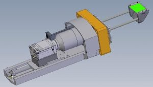
A range of side entry camera mounts which optimise the signal quality from a stingray camera. This mechanism features faster decay phosphor, optimised optical coupling, special lens and reduced background light contamination. Additionally, the camera is mounted perpendicular to the image plane resulting in distortion free diffraction images. These are available for side entry ports (35mm) on most columns.