


Electron Microscopy
SEM, TEM, Electron Diffraction and In-Situ Electron Microscopy
Electron Microscopy (EM) is a microscope technique that uses a beam of electrons to produce high resolution imagery.
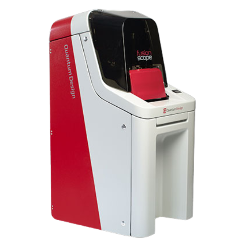
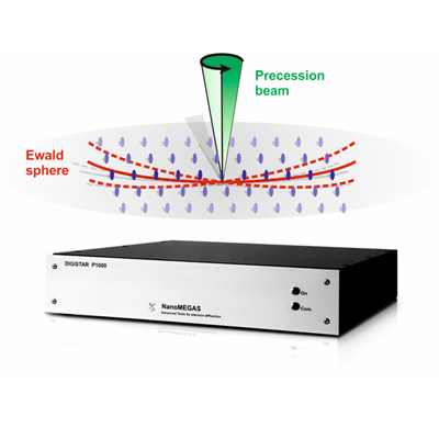

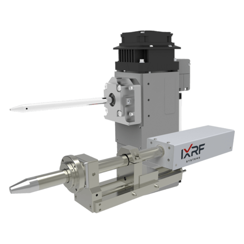

Our suppliers IXRF Systems, NanoMEGAS and QD FusionScope offer a range of tools and equipment including scanning electron microscopes (SEM), transmission electron microscopes (TEM), tools for electron diffraction and in-situ electron microscopy.
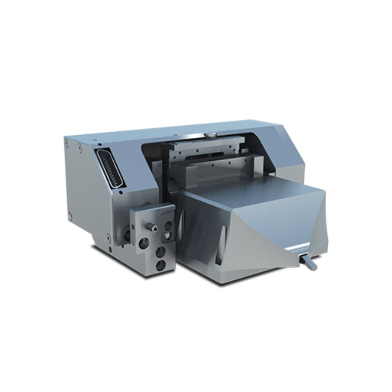
We offer a number of products to enhance your Electron Microscopy capabilities. Our team has many years of experience in Electron Microscopy applications and we can discuss with you your research needs and provide the best solution to match your experiment. All of our products are compatible with the major Electron Microscopy manufacturers and are provided with software to collect and analyse your data.

