


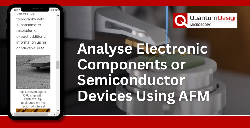
Detailed location and analysis of nanometer-sized structures is a challenging and time-consuming task for all AFM operators. The size reduction in recent generations of transistors creates especially high demands on quality control and failure analysis.
By combining the complementary strengths of AFM and SEM, FusionScope opens the door to a world of new application possibilities.
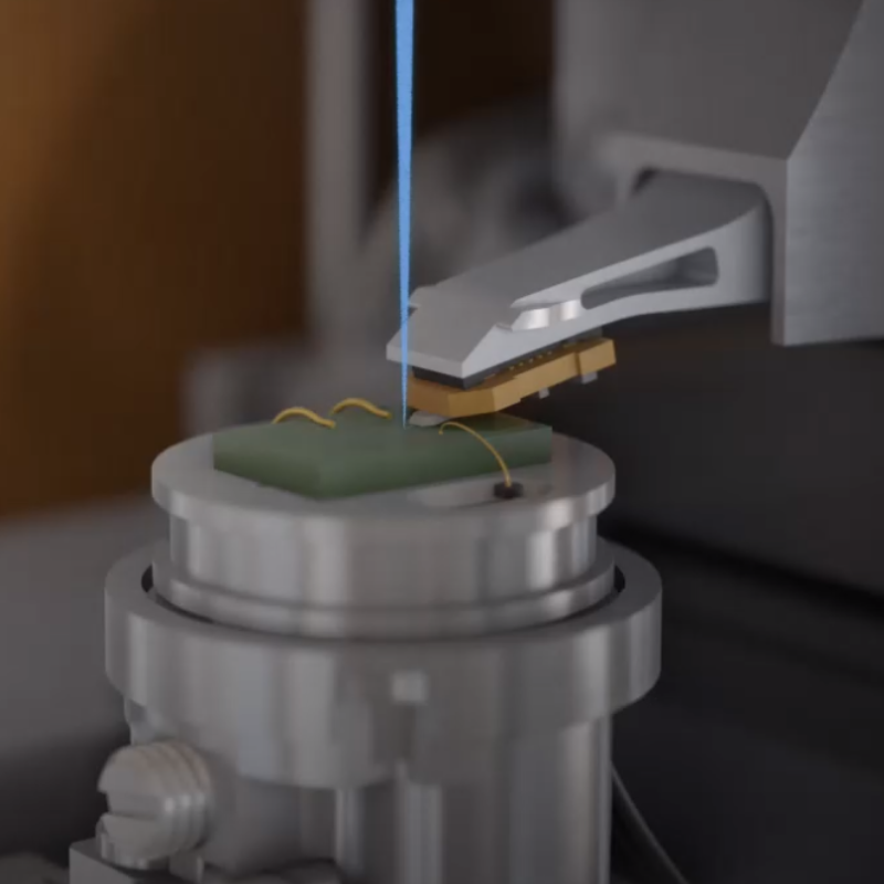
View SEM, AFM and correlative SEM images of a specific area of transistor structures within a CPU chip….
FusionScope is an easy-to-use correlative microscopy platform designed from the ground up to add the benefits of SEM imaging to a wide range of AFM measurement techniques.
Combine the complementary strengths of AFM and SEM like never before! The FusionScope fully integrates a wide range of advanced AFM measurement techniques with the benefits of SEM imaging. Seamlessly image your sample, identify areas of interest, measure your sample, and combine your imaging data in real time.
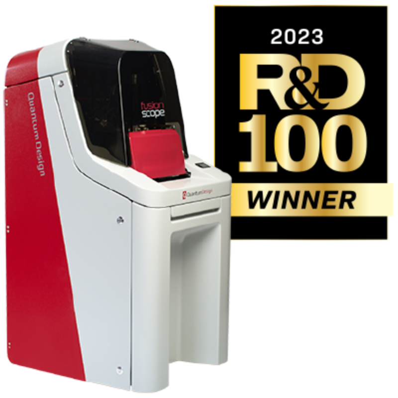
FusionScope™ from QD Microscopy
Easy to use Correlative AFM/SEM Microscopy Platform
More Semiconductor Information in our Magazine
There’s loads of articles, case studies and product information in our Semiconductors magazine.. check it out here.

Any questions about your semiconductor research?
Get in touch with our Techical Product Manager to find out what the FusionScope can do for you.


