
- Features
- Options
- Specifications
- Downloads
- Related Products
- Back To Spectroscopy
- Back To Optics
- Back To Hyperspectral
- Back To Cameras
- Back To X-Ray
- Back To Light Measurement
- Back To Characterisation
- Back To Electron Microscopy
- Back To Magnetometry
- Back To Ellipsometers
- Back To Cryogenics
- Back To Lake Shore
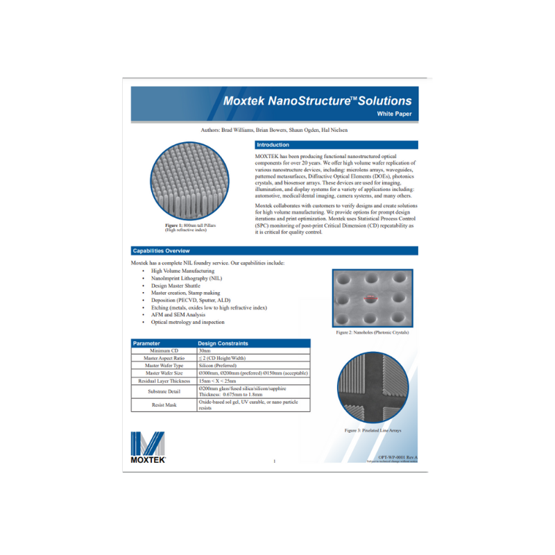
Moxtek NanoStructure Solutions™
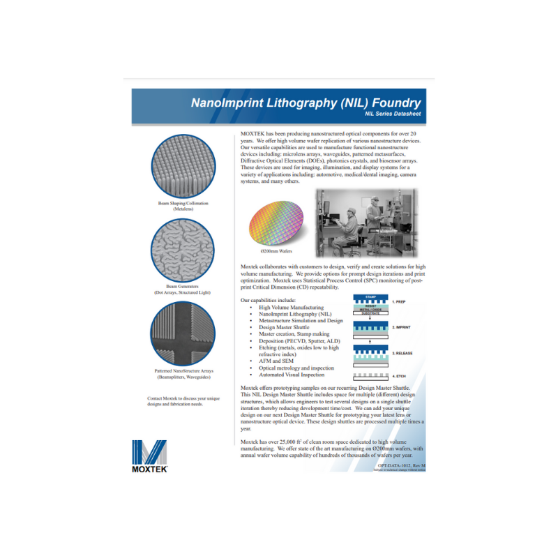
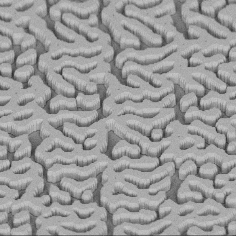
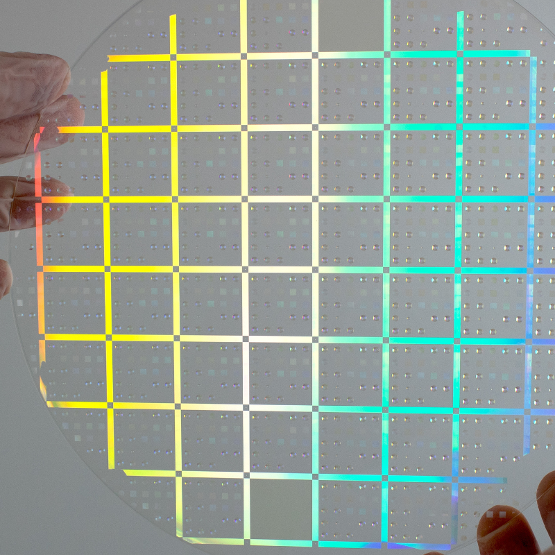
MOXTEK has been producing nanostructured optical components for over 20 years. They offer high volume wafer replication of nanostructure devices on Ø200mm wafers. Moxtek’s versatile capabilities are used to manufacture functional metasurfaces including: metalens, meta-optical elements (MOE), diffractive optical elements (DOE), patterned nanostructures, waveguides, photonics crystals, and biosensor arrays. These devices are used for imaging, illumination, and display systems for a variety of applications including: automotive, medical/dental imaging, camera systems, and many others.
Moxtek collaborates with customers to design, verify and create solutions for high volume manufacturing. We provide options for prompt design iterations and NanoImprint Lithography (NIL) optimisation. Moxtek uses Statistical Process Control (SPC) monitoring of post-print Critical Dimension (CD) repeatability.
Moxtek offers prototyping samples on their recurring Design Master Shuttle. This NIL Design Master Shuttle includes space for multiple (different) design structures, which allows engineers to test several designs on a single shuttle iteration thereby reducing development time/cost. Moxtek can add your unique design on our next Design Master Shuttle for prototyping your latest lens or nanostructure optical device. These design shuttles are processed multiple times a year.
MANUFACTURING CAPABILITIES
- High Volume Manufacturing
- Prototyping Options
- NanoImprint Lithography (NIL)
- Design Master Shuttle
- Master creation, Stamp making
- Deposition (PECVD, Sputter, ALD)
- Etching (metals, oxides low to high refractive index)
- AFM and SEM
- Optical metrology and inspection
CONFIGURABLE PARAMETERS
- Minimum CD: 30nm
- Master Aspect Ratio: ≤ 2 (CD Height/Width)
- Master Wafer Type: Silicon (Preferred)
- Master Wafer Size: Ø300mm, Ø200mm (preferred) Ø150mm (acceptable)
- Residual Layer Thickness: 15nm < X < 25nm
- Substrate Detail: Ø200mm glass/fused silica/silicon/sapphire Thickness: 0.675mm to 1.8mm
- Resist Mask: Oxide-based sol gel, UV curable, or nano particle resist
Profile

Profile
Profile

Profile

Profile

Profile

Profile

Custom Metalens Foundry Service | Visible and IR Wavelengths
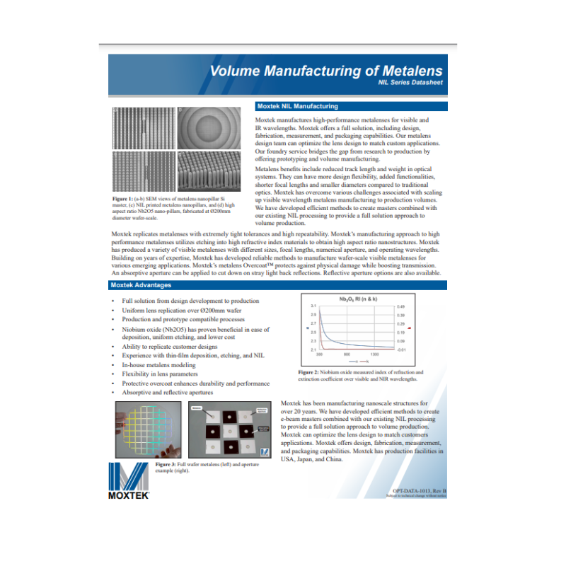
Moxtek manufactures high-performance metalenses for visible and IR wavelengths. Moxtek offers a full solution, including design, fabrication, measurement, and packaging capabilities. Our metalens design team can optimise the lens design to match custom applications. Our foundry service bridges the gap from research to production by offering prototyping and volume manufacturing.
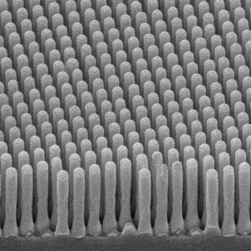
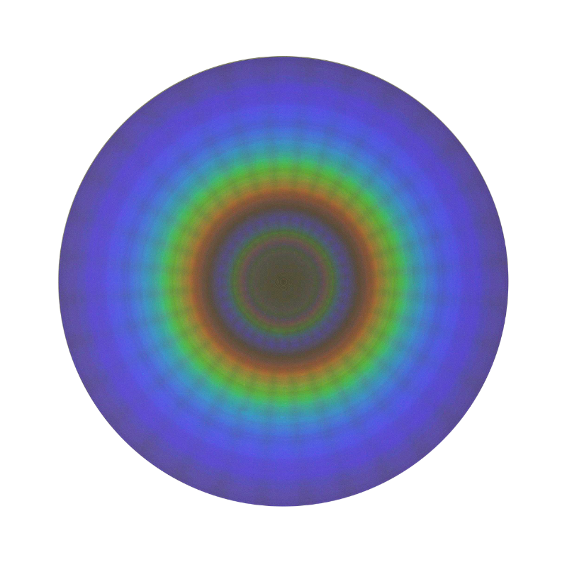
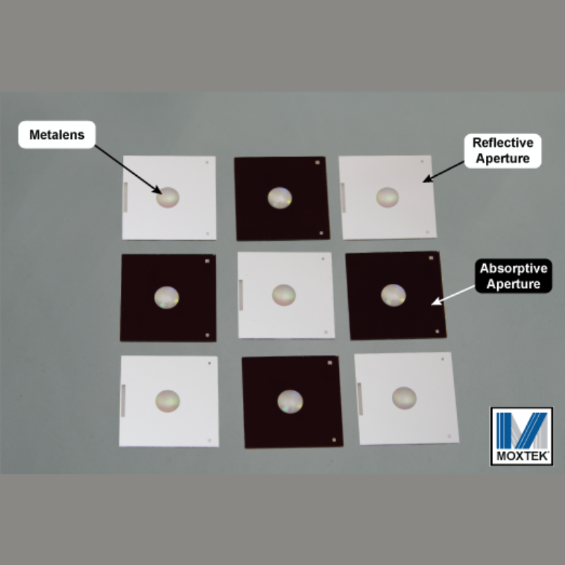
Metalens benefits include reduced track length and weight in optical systems. They can have more design flexibility, added functionalities, shorter focal lengths and smaller diameters compared to traditional optics. Moxtek has overcome various challenges associated with scaling up visible wavelength metalens manufacturing to production volumes. We have developed efficient methods to create masters combined with our existing NIL processing to provide a full solution approach to volume production. Moxtek replicates metalenses with extremely tight tolerances and high repeatability. Moxtek’s manufacturing approach to high performance metalenses utilises etching into high refractive index materials to obtain high aspect ratio nanostructures. Moxtek has produced a variety of visible metalenses with different sizes, focal lengths, numerical aperture, and operating wavelengths. Building on years of expertise, Moxtek has developed reliable methods to manufacture wafer-scale visible metalenses for various emerging applications. Moxtek’s metalens Overcoat™ protects against physical damage while boosting transmission. An absorptive aperture can be applied to cut down on stray light back reflections. Reflective aperture options are also available. See our manufacturing parameters below. For more information:
- Uniform lens replication over Ø200mm wafer
- Production and prototype compatible processes
- Niobium oxide (Nb2O5) has proven beneficial in ease of deposition, uniform etching, and lower cost
- Ability to replicate customer designs
- Experience with thin-film deposition, etching, and NIL
- In-house metalens modeling
- Flexibility in lens parameters
- Protective overcoat enhances durability and performance
- Minimum CD: 70nm
- Minimum Space Gap: 70nm
- Thickness: ≤1,000nm
- Aspect Ratio: 12:1
- Meta Materials (preferred): Nb2O5, Al
- Meta Materials (other): Si, SiO2, Si3N4
- Substrate Diameter: Ø200mm diameter
- Substrate Thicknesses: 0.7mm to 1.6mm thick
- Substrate Types: Display glass, Fused Silica, Silicon, Sapphire