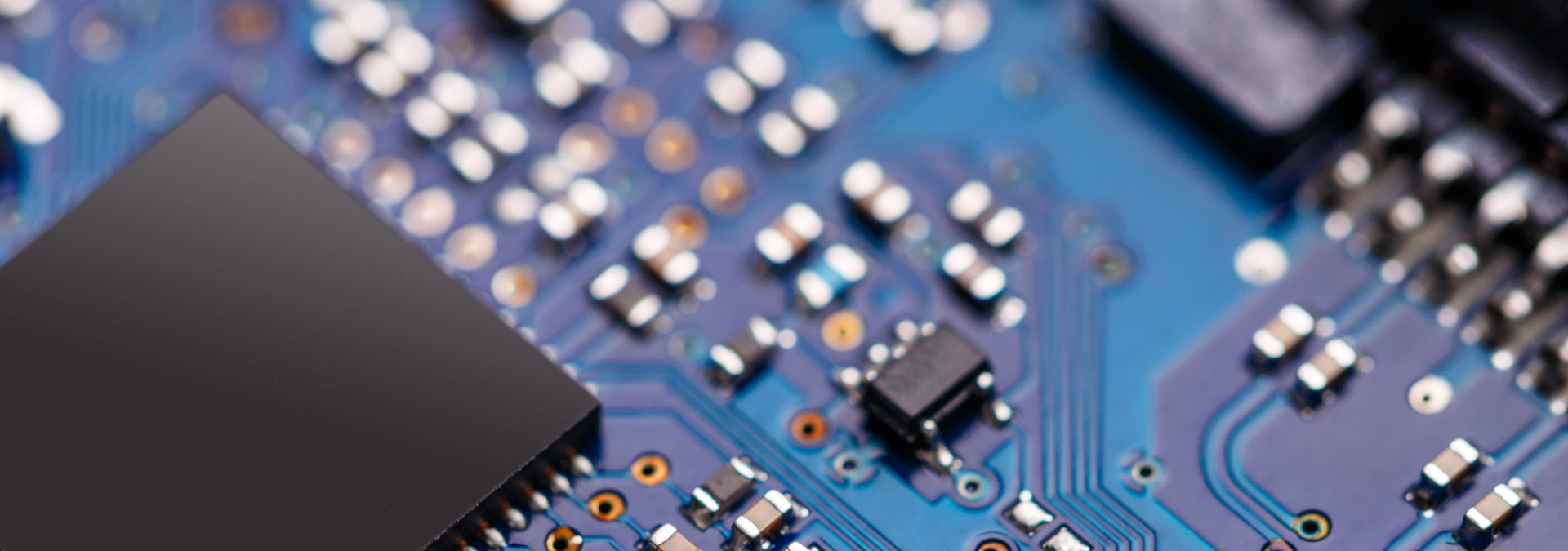
High tech instrumentation for the Semiconductor industry
The UK is a global leader in semiconductor chip design. The country will play a key role in developing the industry in the future. QDUKI is ready to assist with the challenges we will face while shaping the development of advanced packing and compound semiconductors.
Quantum Design (QD) has been a leader in high-tech instrumentation for over 40 years with systems such as the MPMS and VersaLab. We have continually added to our product portfolio by acting as distributor for other market leaders who provide solutions for semiconductors, including J. A. Woollam, InfraTec, Sigray, 4D Technology and Lake Shore Cryotronics. This means we can provide our customers with the right solutions for their semiconductor applications.
iXRF Atlas X
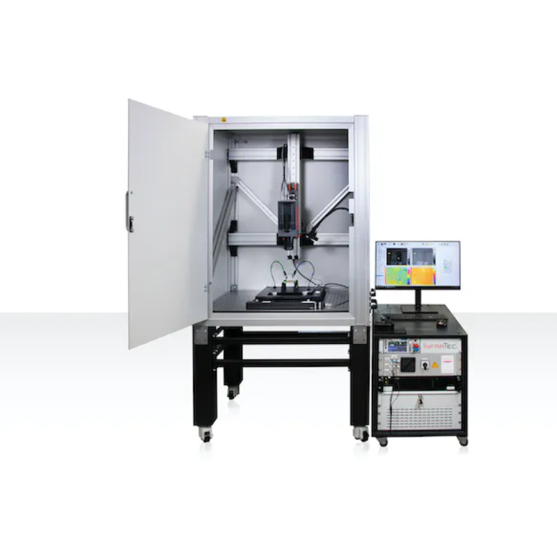
InfraTec E-LIT Electronics / Semiconductor Testing Solution
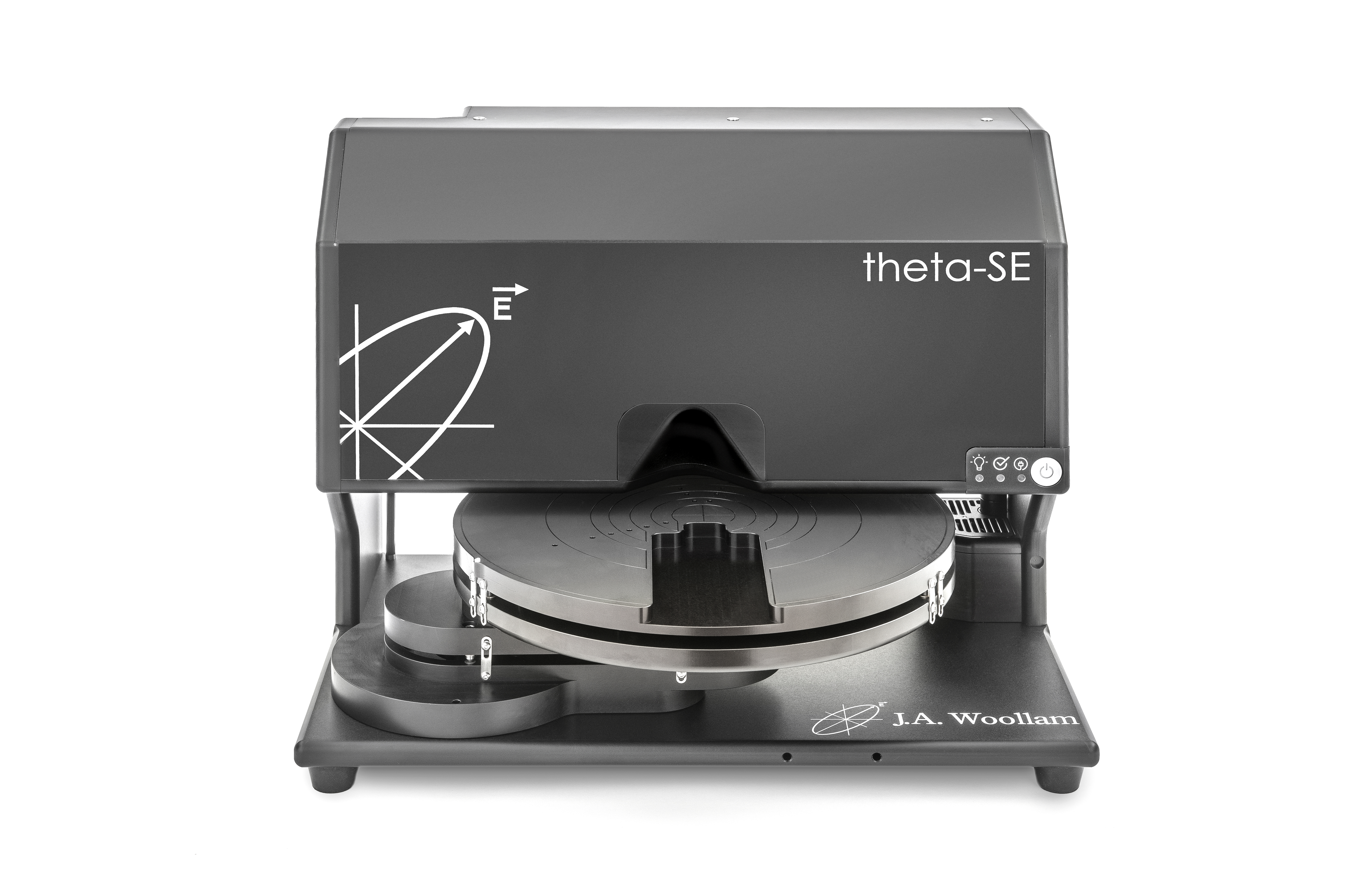
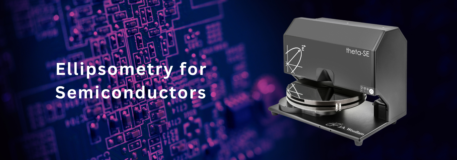
J. A. Woollam theta-SE Spectroscopic Ellipsometer
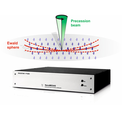
Nanomegas A-Star TEM Orientation Imaging
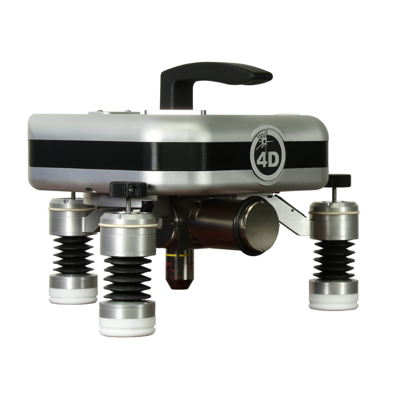
4D Technology NanoCam HD Optical Profiler
Andover Corporation Optical Filters
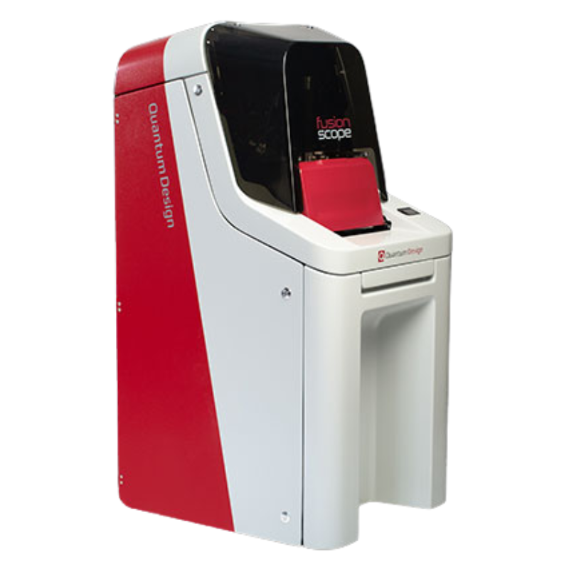
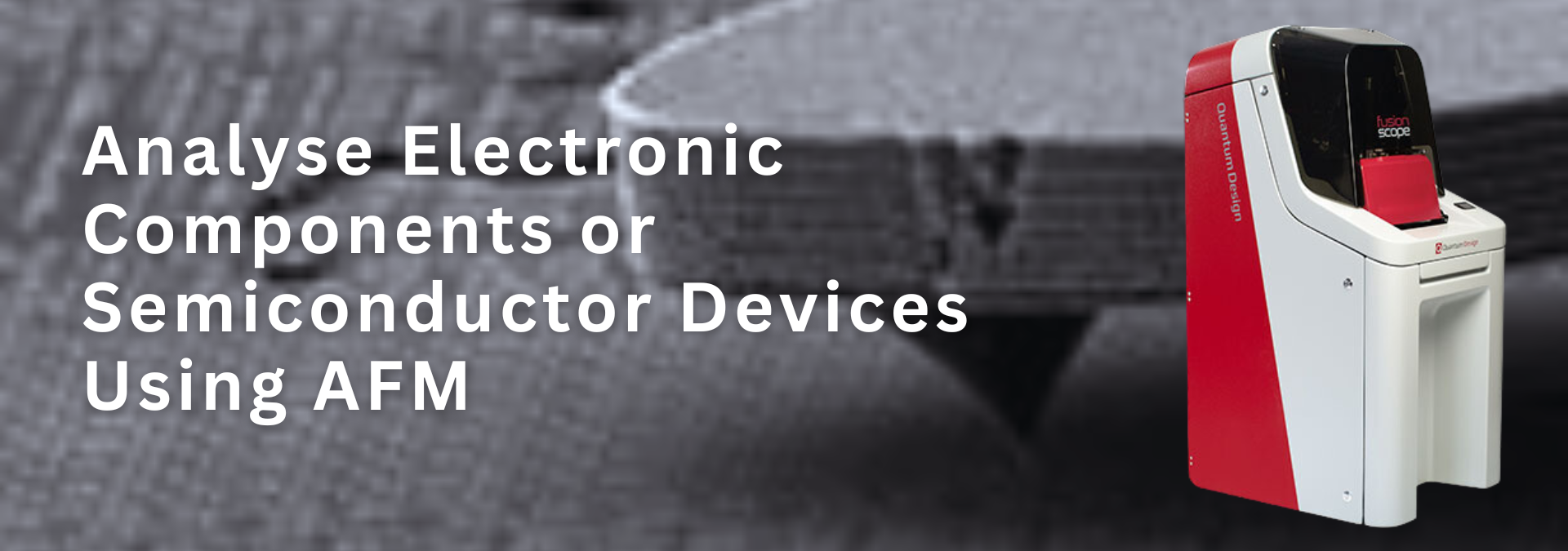
QD Microscopy FusionScope™ Correlative Microscopy Platform
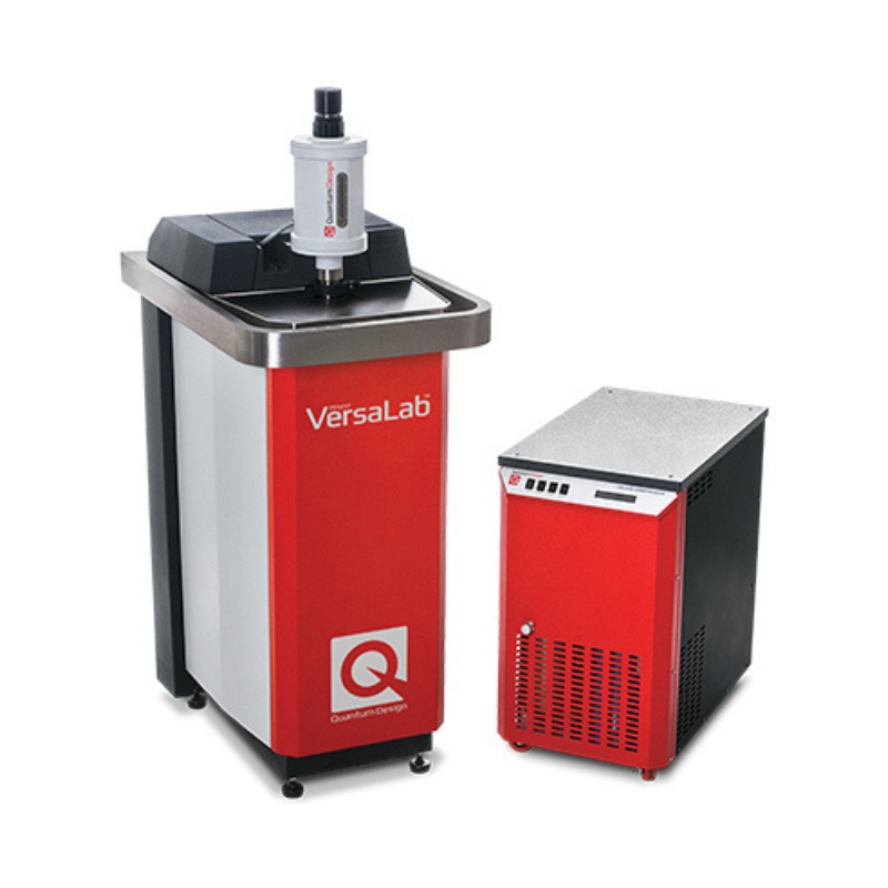
Quantum Design VersaLab™ Measurement System
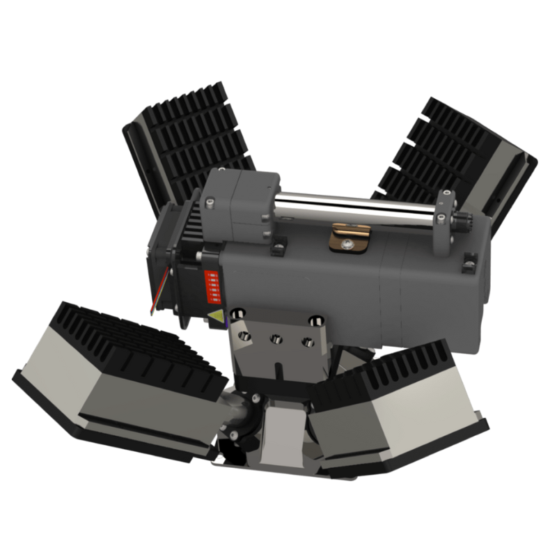
Raptor Photonics Hawk Indigo
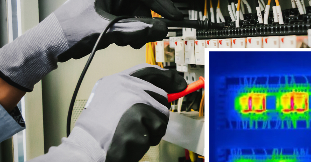
Thermography Solutions for Power Electronics
Precise, Non-contact and High-speed
- Semiconductor testing solution E-LIT
- Thermal analysis of electronic and semiconductor devices
- Modular test bench for online lock-in measurements
- Infrared Cameras for Electronics
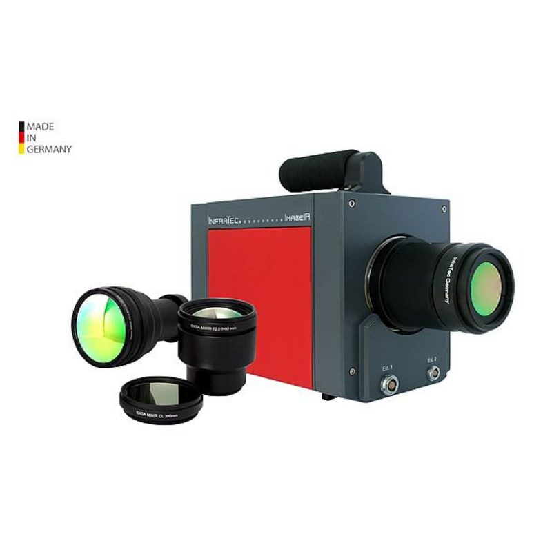
ImageIR® 8300 hp
COMPLEMENTARY EVALUATION OF POTENTIAL BARRIERS IN SEMICONDUCTING BARIUM TITANATE BY ELECTROSTATIC FORCE MICROSCOPY AND CAPACITANCE-VOLTAGE MEASUREMENTS
Electrostatic force microscopy (EFM) was used to directly image the impact of SiO2 content variations on the grain boundary potential barriers in semiconducting BaTiO3-based ceramics. The grain boundary barriers were shown to be significantly thinner and more pronounced as the amount of SiO2 was increased from 0 to 5 mol%. The EFM results were confirmed by capacitance–voltage (C–V) measurements which proofs the accuracy of both methods and highlights their importance for gaining a better understanding of the interrelations between material composition and electrical properties.
ALL APPLICATIONS

Defence and Security

Aerospace

Quantum Science and Technology
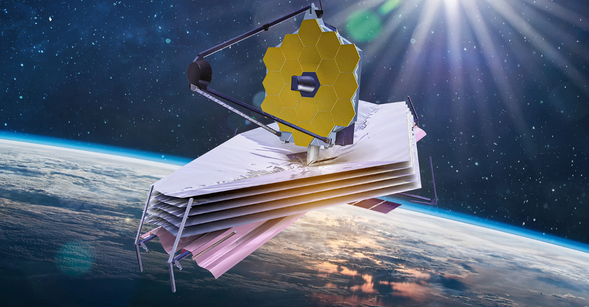
Space and Astronomy
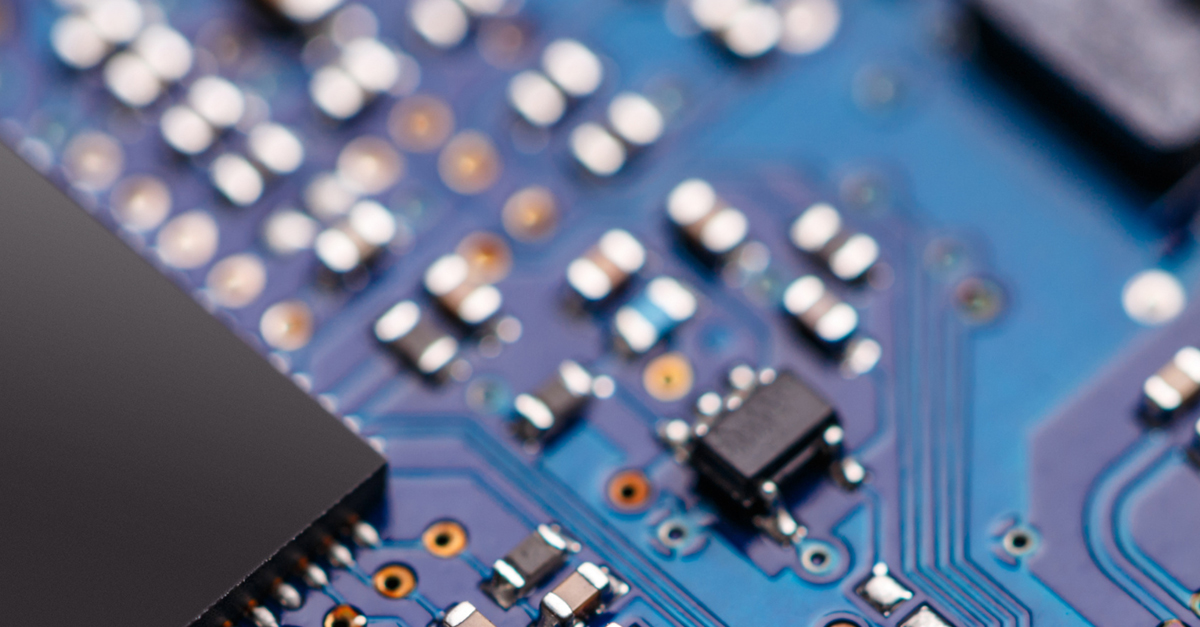
Semiconductors

Agriculture
Non-Destructive Testing