


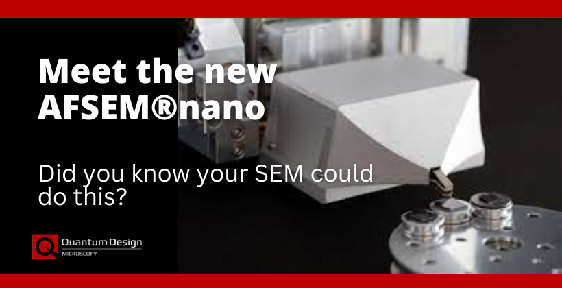
Did you know your SEM could do this?
The new AFSEM®nano from QD Microscopy combines the best of both worlds with AFM in your SEM/FIB
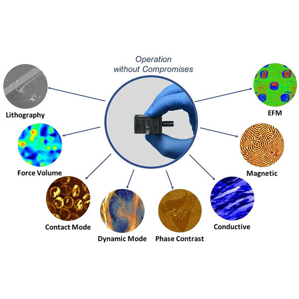
The AFSEM is a fully functional atomic force microscope and therefore is capable of all normal measurement modes expected from a standard AFM. Contact mode, intermittent contact mode, non-contact, force-volume, and phase contrast mode are all available and the user can switch between them easily using the controller software. The advanced modes, namely Conductive AFM (C-AFM), Magnetic Force Microscopy (MFM) and Electrostatic Force Microscopy (EFM) are also available by using the functional probes. Kelvin Probe Force Microscopy (KPFM) and Scanning Thermal Microscopy (SThM) are currently under development.
Features
- World’s smallest AFM insert for your SEM/FIB
- Seamless integration: Measure any sample your SEM/FIB accepts
- Analyse your sample in-situ by AFM and SEM without breaking vacuum
- Correlative microscopy allows you to quickly and easily perform AFM analysis on your area of interest
- Add real 3D topography to your EDX or EBSD data
- Reconstruct 3D nanomechanical properties by FIB-assisted tomography
- Measure electric and magnetic properties inside your SEM with nanometer resolution
Measurement modes:
Standard AFM
In contact mode, the tip is in contact with the surface of the sample and follows the topography closely in the repulsive regime. For contact mode long and soft cantilevers with low force constants are used.
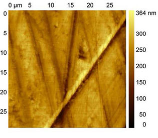
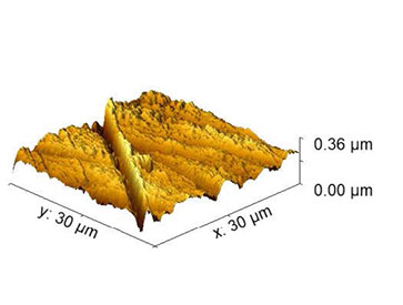
(Figures 1 and 2) AFSEM image of a polymer surface obtained in contact mode.
In intermittent contact mode, also called dynamic mode, the cantilever is oscillated near its resonance frequency. When the tip comes close to the surface, the interaction between the tip and the sample cause the amplitude of the oscillation to change. As the cantilever is scanning over the sample, the height is adjusted to maintain a set cantilever oscillation amplitude. An AFM image is therefore produced by imaging the force of the intermittent contacts of the tip with the surface.
AFSEM image of freestanding graphene membranes obtained in intermittent contact mode.
(Figure 1) Correlative SEM/AFM image of the graphene membranes.
(Figure 2) High-resolution AFM image of a single freestanding graphene membrane.
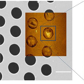
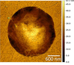
In non-contact mode, the tip of the cantilever does not contact the sample surface. The tip is oscillated only with a very small amplitude and is affected only by the long-range forces and therefore neither sample degradation nor tip degradation occur.
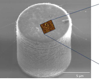
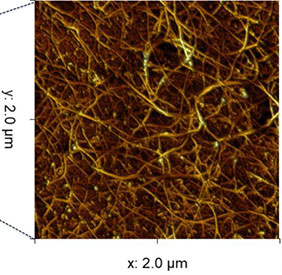
AFSEM image of silicon micro-pillar surface obtained in non-contact mode
(Figure 1) Correlative SEM/AFM image of the micro-pillar surface.
(Figure 2) High-resolution AFM image of the micro-pillar surface decorated with nano-wire network.
In force-volume mode, force measurements are combined with topographic imaging. Typical AFM images depict the topography of a surface by measuring the action of a feedback loop to maintain a constant tip/sample interaction as the tip is scanned across the surface. The force volume data set combines nearly simultaneously measured topographic and force information into a single data set allowing the microscopist to test for correlations between forces and surface features.
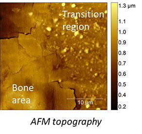
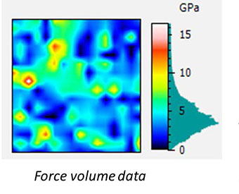
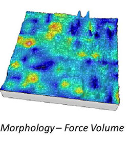
AFSEM image of bone sample with a partially dissolved implant obtained in force volume mode.
(Figure 1) AFM Topography image of the bone area and transition region, where the implant is partially dissolved.
(Figure 2) Force volume data of the same area.
(Figure 3) Overlay of topography and force volume data.
C-AFM
Conductive AFM mode (C-AFM) measures the conductive properties of the sample using a conductive tip. The conductive tips used by AFSEM are produced using Focused Electron Beam Induced Deposition (FEBID) and are made of pure Platinum, which ensures their high stability and longevity. There is no extra module needed for C-AFM measurements.
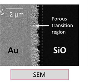
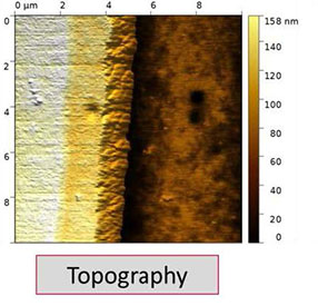
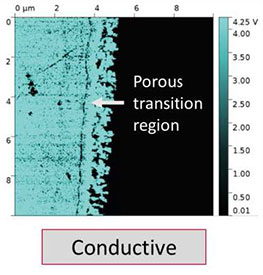
AFSEM C-AFM image of a gold electrode on a silicon substrate.
(Figure 1) SEM image of the region of interest displaying the gold electrode with a porous transition region at the edge of the electrode structure.
(Figure 2) AFM Topography image of the electrode structure.
(Figure 3) C-AFM image of the electrode structure that reveals the highly conducting gold electrode as well as the non-conducting silicon surface region.
MFM
Magnetic AFM Mode (MFM) is used to study the magnetic properties of magnetic materials using a magnetic tip. The conductive tips used by AFSEM are produced using Focused Electron Beam Induced Deposition (FEBID) and are made of Fe/Co. AFSEM uses a dual pass technique: A first scan images the topography. Then a second scan, where the tip follows the measured topography with a set distance above the sample, measures the phase shift due to magnetic force between tip and sample. By default, the AFSEM is capable of this so called “lift-mode”.
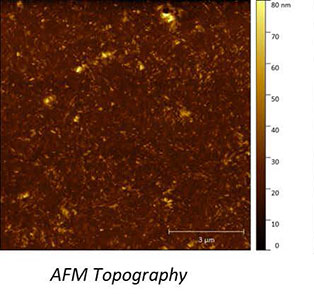
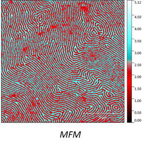
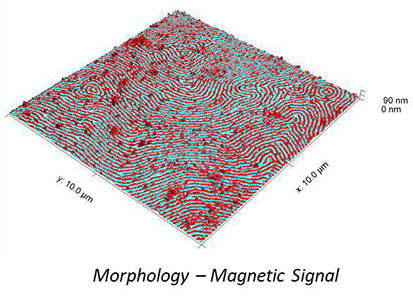
AFSEM MFM image obtained on a multilayered magnetic sample.
(Figure 1) AFM Topography.
(Figure 2) MFM Phase contrast revealing the different magnetic domains.
(Figure 3) Overlay of topography and magnetic signal.

Discover what you could be doing with your SEM.
Contact our Technical Product Manager, Dr. Satyam Ladva by email or call (01372) 378822.


