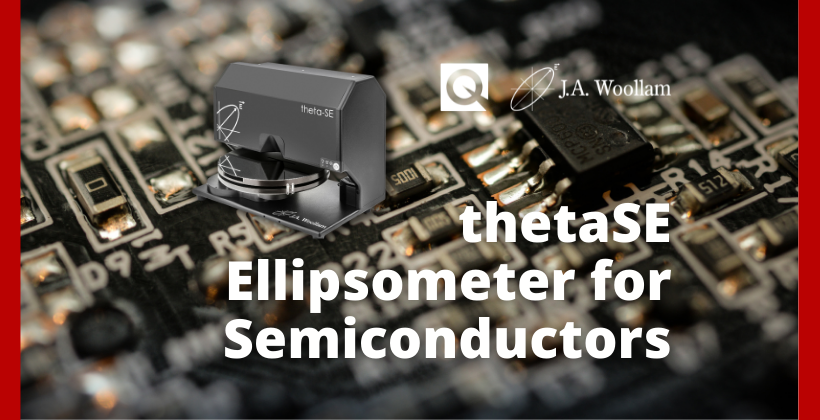
Since the 1960s, as ellipsometry developed to provide the sensitivity necessary to measure nanometer-scale layers used in microelectronics, interest in ellipsometry has grown steadily. Today, the range of its applications has spread to the basic research in physical sciences, semiconductor and data storage solutions, flat panel display, communication, biosensor, and optical coating industries. Here we take a look specifically at the J A Woollam thetaSE ellipsometer and its uses for the semiconductor industry.

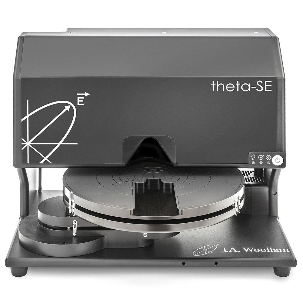
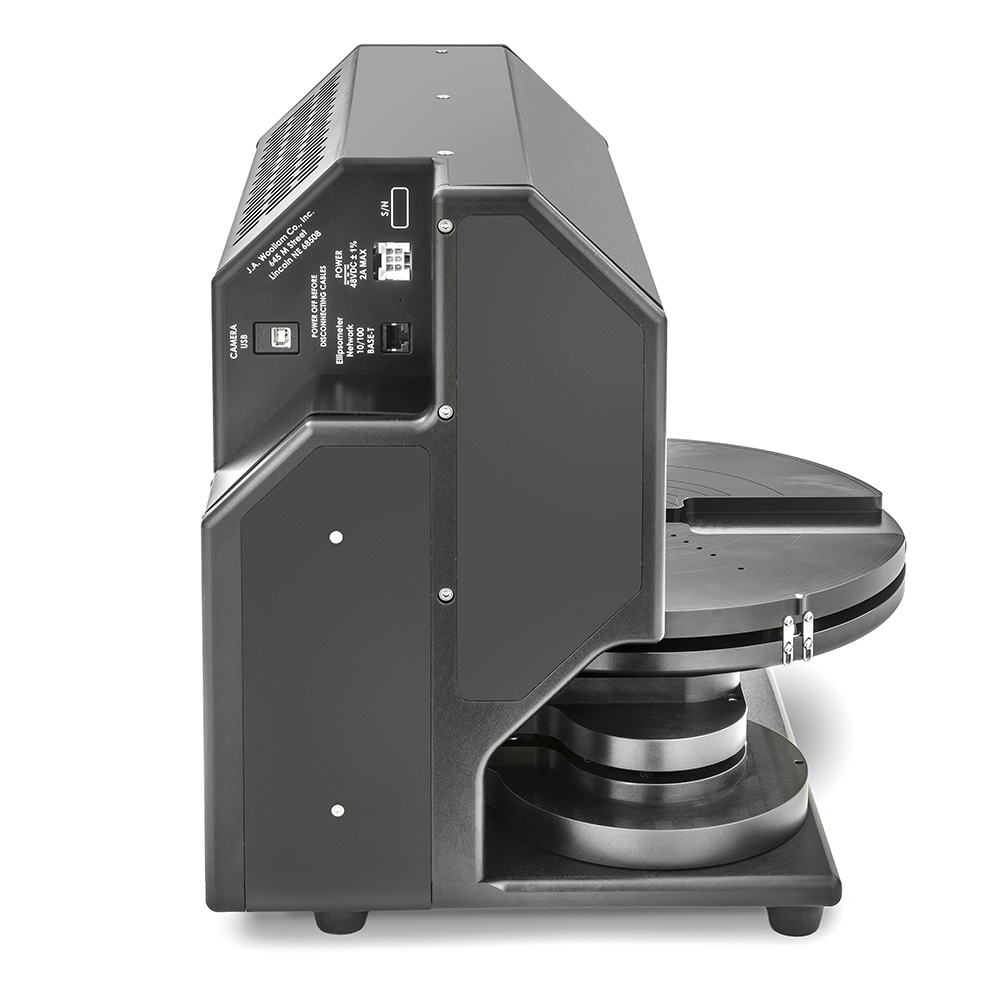
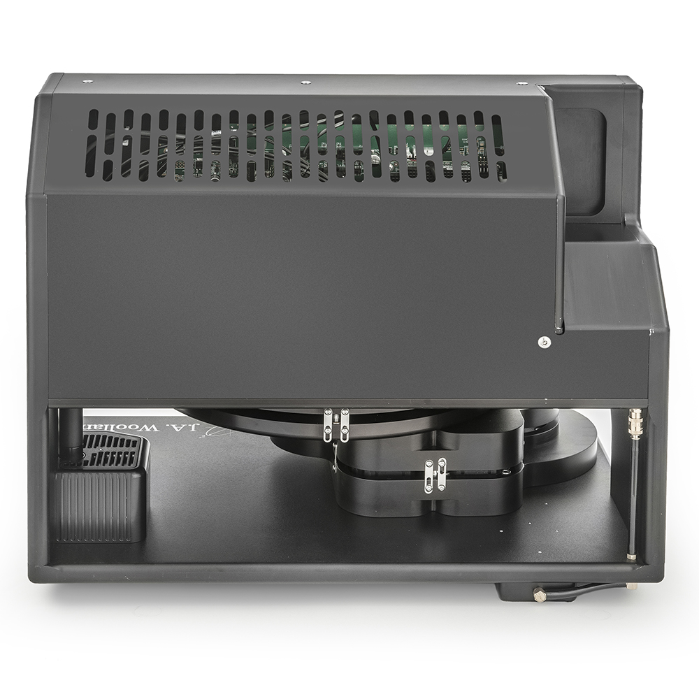
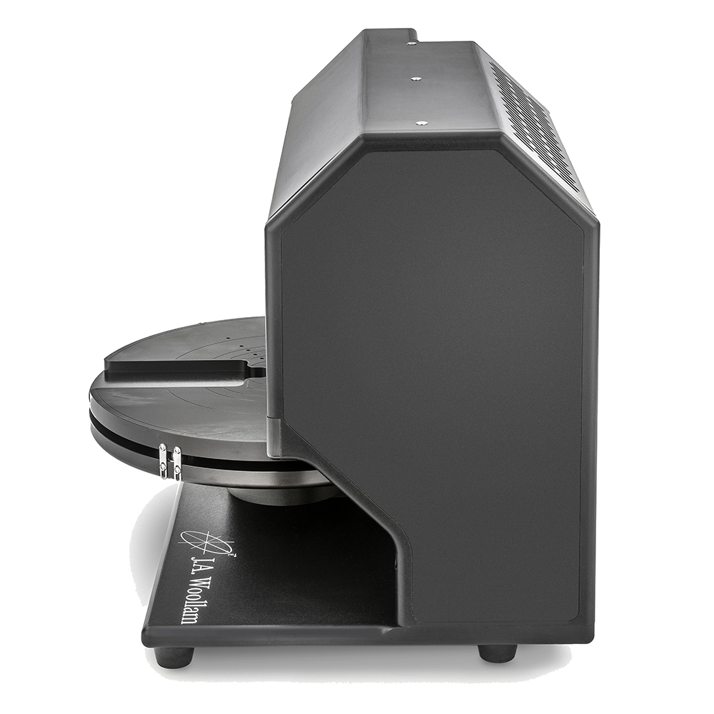
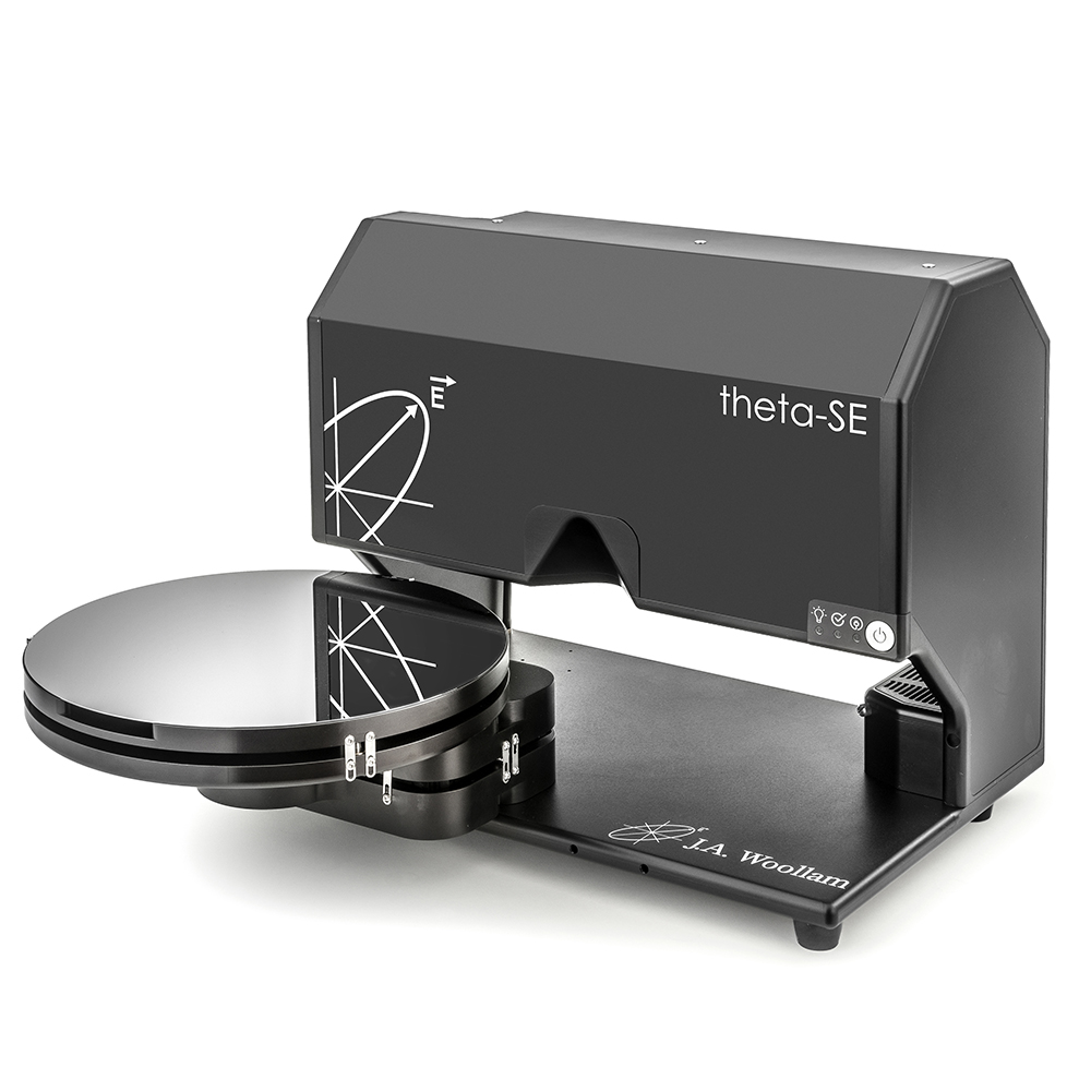
The theta-SE is a push-button spectroscopic ellipsometer for characterising thin film uniformity. It features advanced ellipsometry instrumentation in a compact package at an affordable price.
Results at Wavelengths of Interest for a Desired Application
For many applications, optical properties are desired at specific wavelengths. For example, the semiconductor industry is interested in lithography which requires ellipsometry measurements in the UV region (157nm, 193nm, 248nm,…). The display industry is interested in the visible spectrum. Optical coatings require measurement at their design wavelengths, whether at visible, near infrared or even mid-infrared wavelengths. Woollam Spectroscopic Ellipsometers cover the spectral range from 33 microns to 140nm. This range offers an incredible flexibility that can meet almost any application requirement.
Semiconductor Industry
- Dielectrics (oxides, nitrides, carbides)
- Polymers (Low-Dielectric constant)
- Polysilicon
- Multilayers (ONOPO, SOI,…)
- Lithography Applications
- Photoresists
- Antireflective coatings
- Photomasks
- Compound Semiconductors
Technical Papers on Semiconductors:
| Ellipsometry Characterization of Bulk Acoustic Wave Filters Authors: E. Nolot, A. Lefevre, J. Hilfiker Phys. Stat. Sol. (c) 5, No.5, 17, (2008) 1168-1171. | |
| Spectroscopic Ellipsometry (SE) for Materials Characterization at 193 and 157nm Authors: J. Hilfiker, F. G. Celii, W. D. Kim, E. A. Joseph, C. Gross, T. Y. Tsui, R. B. Willecke, J. L. Large, and D. A. Miller Semiconductor Fabtech, 17, (2002) 87-91. | |
| Immersion Fluids for Lithography: Refractive Index Measurement Using Prism Minimum Deviation Techniques Authors: R. Synowicki, G. Pribil, G. Cooney, C. Herzinger, S. Green, R. H. French, M. K. Yang, M. F. Lemon, J. H. Burnett, and S. Kaplan Semiconductor Fabtech, 22, (2004) 55-58. | |
| Spectroscopic Ellipsometry as a Potential In-Line Optical Metrology Tool for Relative Porosity Measurements of Low- K Dielectric Films Authors: N. V. Edwards, J. Vella, Q. Xie, S. Zollner, D. Werho, I. Adhihetty, R. Liu, T. Tiwald, C. Russell, J. Vires, and K. H. Junkerd Mat. Res. Soc. Symp. Proceedings, 697, (2002) P4.7.1-P4.7.6. | |
| Spectroscopic Ellipsometry Analysis of InGaN/GaN and AlGaN/GaN Heterostructures Using a Parametric Dielectric Function Model Authors: J. Wagner, A. Ranakrishnan, H. Obloh, M. Kunzer, K. Köhler, and B. Johs MRS Internet J. Nitride Semicond. Res. XX, WY.Y, (2000). |
WHY A THETA-SE?
Fully Integrated
The theta-SE comes equipped with 300 mm sample mapping, small-spot measurement beam, fast sample alignment, look-down camera and our latest Dual-Rotation ellipsometer technology. The theta-SE has everything you need to measure the spatial uniformity of your film thickness and optical properties.
High Speed
Sample throughput is optimised by using fast point-to-point translation, high-speed sample alignment and Dual-Rotation ellipsometer technology for continuous data collection.
Compact
The patented, Dual-Theta rotation stage enables full, 300 mm mapping in a small, table-top instrument. The instrument footprint is only slightly larger than a 300 mm wafer.
User Friendly
Automated data analysis and built-in reporting enables push-button operation and quick access to measurement results.
Affordable
The theta-SE delivers the power of spectroscopic ellipsometry and 300 mm uniformity mapping at a reasonable price.
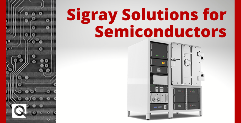
If you need Semiconductor solutions…
… you ll love the Sigray Apex
Sub-Micron 3D X-ray In Minutes
This special 3D X-ray Microscope is designed specifically to analyse large wafer samples, up to 300 mm, and for use in advanced semiconductor packaging and failure analysis.