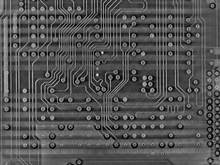
Sigray’s x-ray solutions include 3D x-ray microscopes and microXRF systems in vacuum environments. These systems are used for a range of semiconductor applications, including everything from inspection of wafer contamination and silicon-side process monitoring to failure analysis of packaging.
Packaging Failure Analysis – Absorption Contrast
Sigray has developed a revolutionary new approach to failure analysis with a patent-pending acquisition geometry for flat samples. Using this method, acquisition times of 10X faster than the next leading competitor at submicron spatial resolutions can be achieved. The Sigray Apex XCT is special 3D X-ray Microscope is designed specifically to analyse large wafer samples, up to 300 mm, and for use in advanced semiconductor packaging and failure analysis.
App Note –
Front-end-of-the-line (FEOL) Process Monitoring
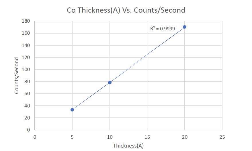
Sigray’s AttoMap XRF has been adopted by leading semiconductor companies for inspection of FEOL processes due to its accurate quantification and small spot sizes of 3-20 µm, allowing focusing of the beam completely within a 40 µm test pattern. The high sensitivity of the AttoMap enables quantitative analysis of trace levels of dopants and has demonstrated down to sub-Angstrom equivalent thickness.
Organic Contaminants and Trace Low-Z Elements
There is a general misperception that quantification of low atomic number (Z) elements such as B, C, O, and N at minor to trace levels is not achievable with microXRF at high resolutions. AttoMap-310 features a high vacuum chamber and a patented Si-based x-ray source that provides optimal illumination for low atomic number elements. Information on B doping and organic contamination can be achieved at excellent resolution (10-100 µm).
You may also like: