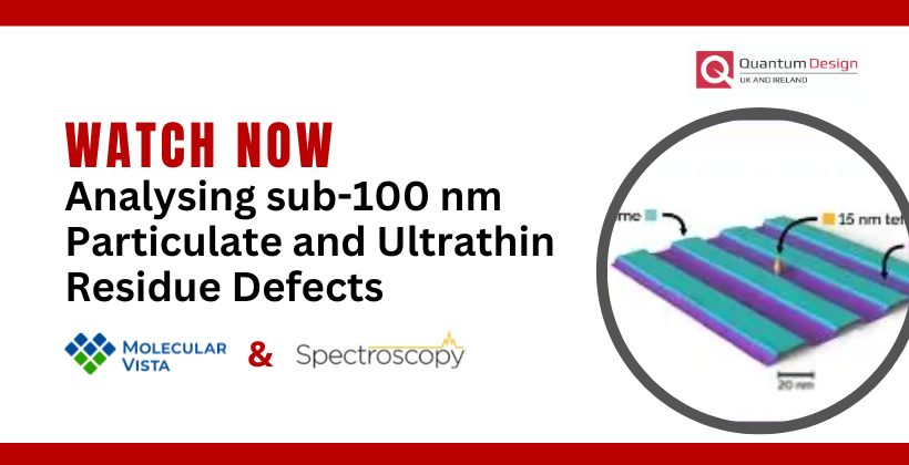
You can now watch a recent online event from our partners Molecular Vista and Spectroscopy Magazine on analysing sub-100 nm particular and ultrathin residue defects.
Most people don’t think it is possible to chemically identify molecules at the nanoscale. However, IR PiFM has the sensitivity and spatial resolution required to name the compound of sub–100-nm defects and directly visualise monolayers based on their molecular vibrations.

Advanced semiconductor processes require clean and properly treated surfaces, free of particulate and residue defects. While atomic species can be identified on these defects via EDS , organic and inorganic compounds cannot be named if they are smaller than ~ 200 nm. While atomic force microscopes (AFMs) are utilised for characterising post-CMP topography, they cannot detect ultrathin and conformal residues or chemically identify contaminants on a surface. By combining infrared spectroscopy with an AFM, photo-induced force microscopy (PiFM) is able to achieve resolutions better than EDS and provide molecular identities rather than atomic identities.
The high spatial resolution (< 5 nm) and surface sensitivity (< 20 nm) provide, for the first time, the ability to chemically name organic and inorganic nanoparticles or monolayer residues.
PiF-IR nano-spectra can be used to name compounds at precise locations, and PiFM chemical maps can show the distribution of different chemical components across the AFM topography. Whether a particle or ultrathin film is intended or unintended, no other technique provides the direct visualisation of surface chemistry like PiFM and PiF-IR.
The yield of a semiconductor process depends on knowing precise information about a surface—if a film exists, what it is, and how it is dispersed on the surface. If a particle exists, what it looks like and what it is made of. This webinar will demonstrate the capabilities of PiFM and PiF-IR and allow you to ask the experts for insight on solving problems you face today.
Key Learning Objectives:
- Existence of IR PiFM for AFM plus IR spectroscopy/mapping with sub–5-nm spatial resolution
- Understand the applications of IR PiFM in semiconductor metrology
- Review application examples in naming sub–100-nm particulate defects and ultrathin conformal surface contaminants

Speaker:
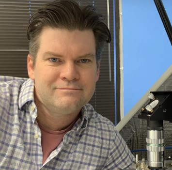
Derek Nowak, PhD
VP, Technical Operations
Molecular Vista
Ideal for:
- Researchers in failure-analysis labs in semiconductor-related companies
- Users of KLA’s Surfscan and other defect-finding instruments
- Advanced packaging (copper-copper hybrid bonding) process engineers
- EUV and other advanced lithographic process engineers

Want to know more about Molecular Vista?
Get in touch with our Technical Director, Dr. Shayz Ikram, by email below or call (01372) 378822.


