


Join this informative one-hour webinar for a deep dive into advanced nanoscale chemical and structural characterisation.
This session will demonstrate how Photo-induced Force Microscopy (PiFM) can provide unprecedented insights into chemical composition, molecular binding environments and surface topography — enabling a more complete understanding of materials across a wide range of applications.
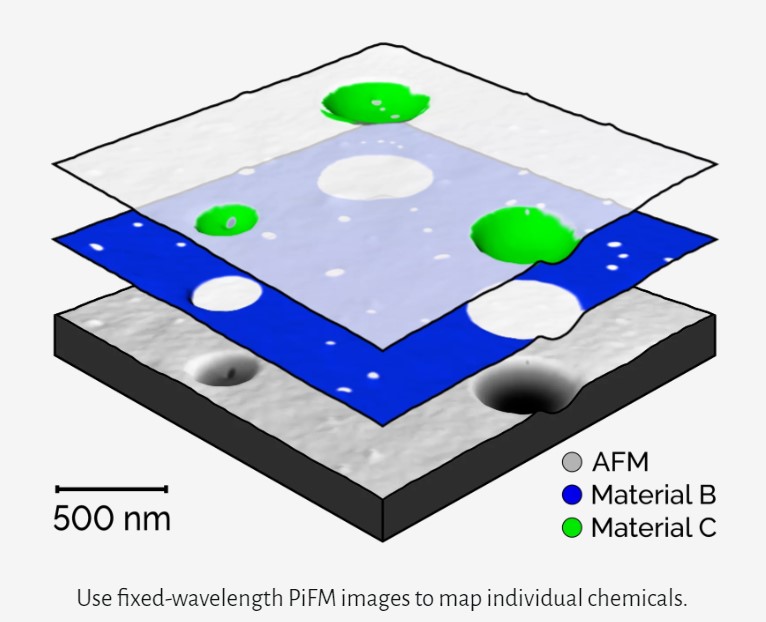
Through practical examples, we will highlight how combing Atomic Force Microscopy with Infrared Spectroscopy allows researchers to probe the same region with multiple modalities, bridging morphology, molecular distribution, and chemical bond information with sub-monolayer sensitivity and sub-5 nm spatial resolution. From complex electronic assemblies to functional coatings and biomedical surfaces, this approach uncovers details that traditional techniques alone cannot resolve.
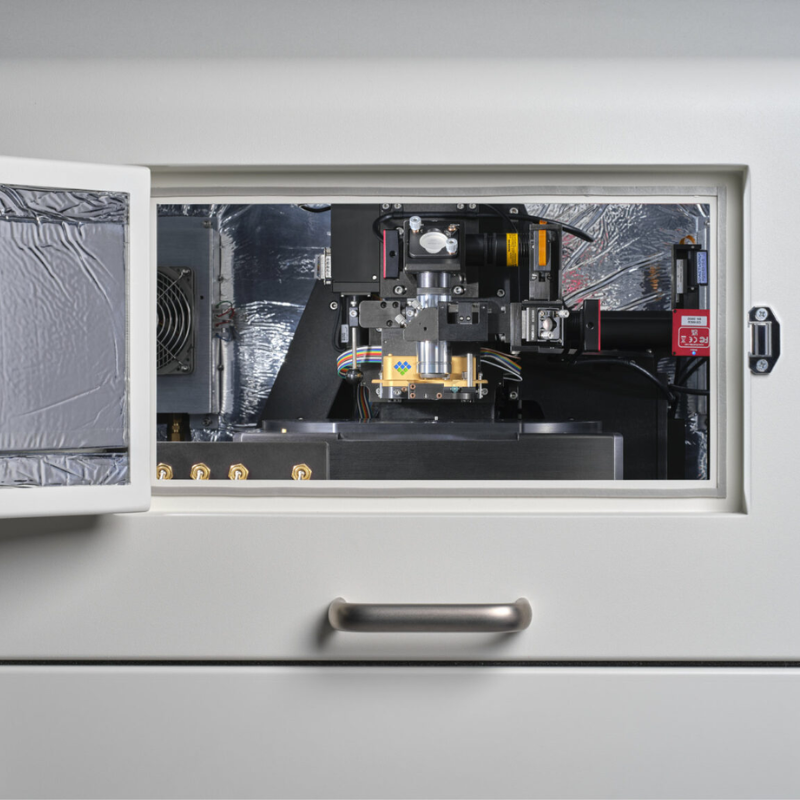
Whether you are working in nanotechnology, semiconductors, data storage, or biomedical devices, this webinar will equip you with tools and strategies to expand your analytical capabilities. You’ll also learn how Covalent integrates PiFM with electron microscopy to deliver fast, high-resolution, and actionable results.
Given its sub-monolayer sensitivity, PiFM is well suited for characterising self-assembled monolayers (SAMs), which are used widely for purposes such as anti-stiction in MEMS devices and hard-disks, surface functionalisation layers in biomedical devices, and inhibitors in selective processes in the semiconductor industry. Currently available techniques such as water contact angle, ellipsometry, and XPS average over a large area, making it impossible to differentiate between a random distribution of clusters versus a continuous monolayer — which can lead to misleading interpretations. In this webinar, we will share results from a nominally 1-nm thick anti-stiction film utilised on hard-disks.
What You’ll Learn
- Limitations of S/TEM-EDS Alone – Recognise that while S/TEM-EDS is a powerful and widely used elemental analysis tool, it does not provide binding or molecular bonding information. This gap makes PiFM essential for a full picture of nanoscale materials.
- Applications in Self-Assembled Monolayers (SAMs) – See case studies on ultrathin functional layers, such as anti-stiction coatings for MEMS and hard-disk technologies.
- Advantages Over Traditional Methods – Learn why contact angle, ellipsometry, and XPS can miss nanoscale variations that PiFM can uniquely resolve.
- Integrated Workflows and Examples – Explore how PiFM enables nanoscale workflows to study the same region with multiple tools, delivering deeper insights into morphology and chemistry.
Live Q&A Session – Ask your questions directly to Covalent and Molecular Vista’s nanoscale characterisation experts.
Molecular Vista manufactures nano‑IR microscopes and develops PiFM and PiF-IR microscopy and spectroscopy. One billion times better than FTIR* – Get nano‑IR spectra to understand nanomaterials at a level unattainable with conventional FTIR techniques. More Time For Science – Save your time for important work. PiF‑IR spectra are fast and easy to take with no finicky alignments or calibration standards needed.
*FTIR is diffraction limited to a resolution of about (10,000 nm )3 = 1×10¹² nm3 while PiF‑IR has a resolution of less than (10 nm)3 = 1×10³ nm3. Therefore, PiF‑IR is at least 1×10⁹ times more precise.

If you have any burning questions before the event, please do contact our Technical Director, Dr. Shayz Ikram by email below, or call (01372) 378822.


