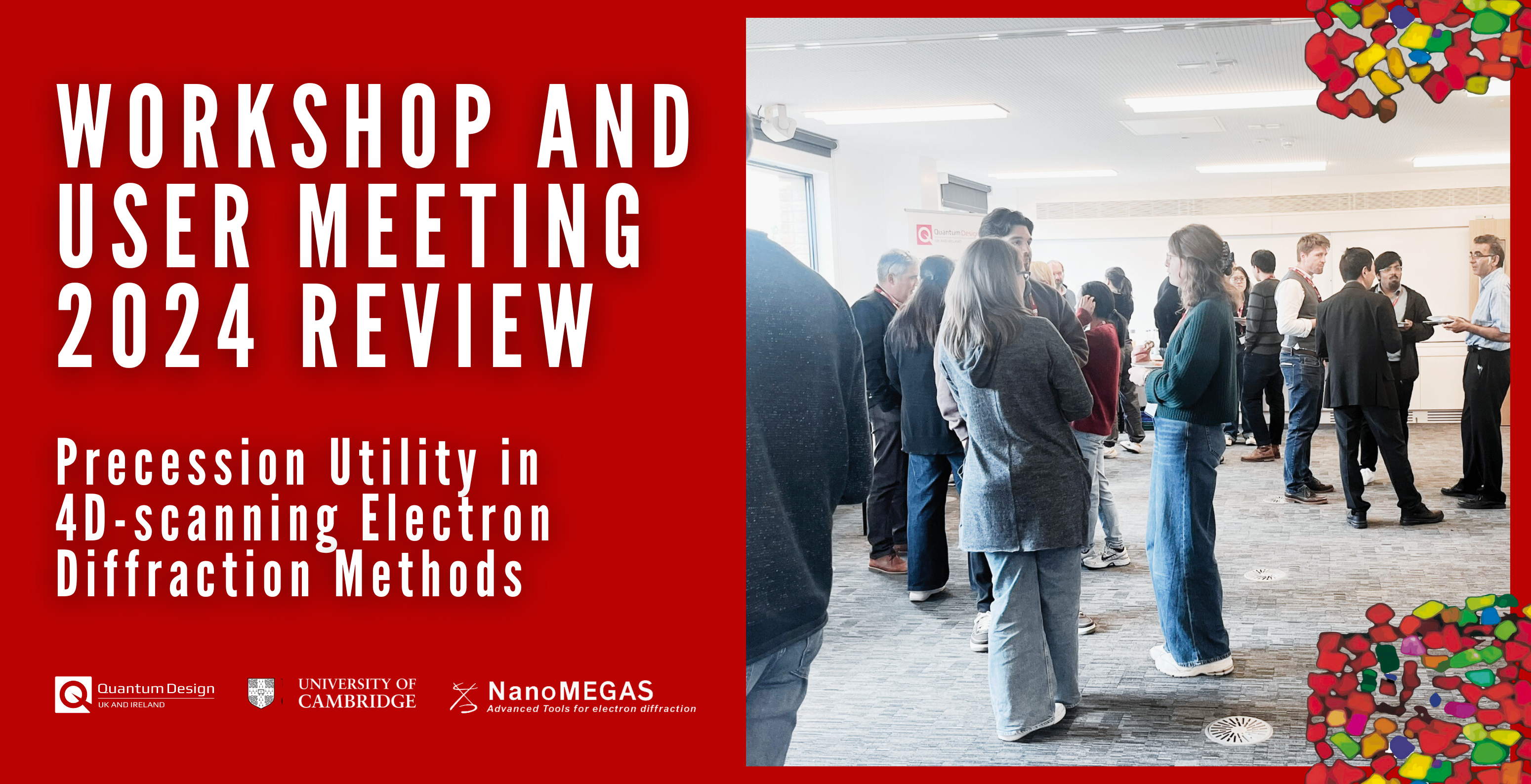
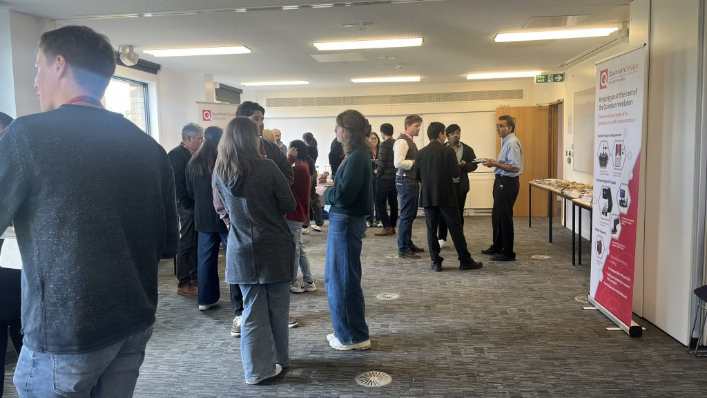
Quantum Design UK and Ireland, NanoMEGAS and the University of Cambridge recently hosted the NanoMEGAS Workshop, celebrating the 30th anniversary of beam precession development in electron diffraction for Transmission Electron Microscopy (TEM). The event was hosted at Cambridge University, an institute with significant historical contributions to beam precession technology. Cambridge University and NanoMEGAS have been pioneers of Precession ED applications, continuously contributing to the systematic development of novel methodologies and applications.
“It was an exceptional experience to participate in the NanoMEGAS Applications of Precession Enhanced Electron Diffraction Workshop, commemorating 30 years of beam precession innovation. Prof. Paul Midgley’s introduction to the historical background and key figures of the beam precession technique was both enlightening and inspiring. The workshop provided invaluable insights into the latest features, developments, and improvements in precession electron diffraction, which are crucial for our ongoing research. Connecting with other users and learning about their applications of NanoMEGAS systems in automated crystal orientation mapping, strain mapping, electron crystallography, and electric-magnetic field mapping was incredibly beneficial. The new advancements shared by Quantum Design UK and Ireland further underscored the significance and future potential of these technologies.”
Dr. Jiahui Qi, Experimental Officer, Electron Microscopy: TEM/FIB, University of Sheffield
Topics Covered
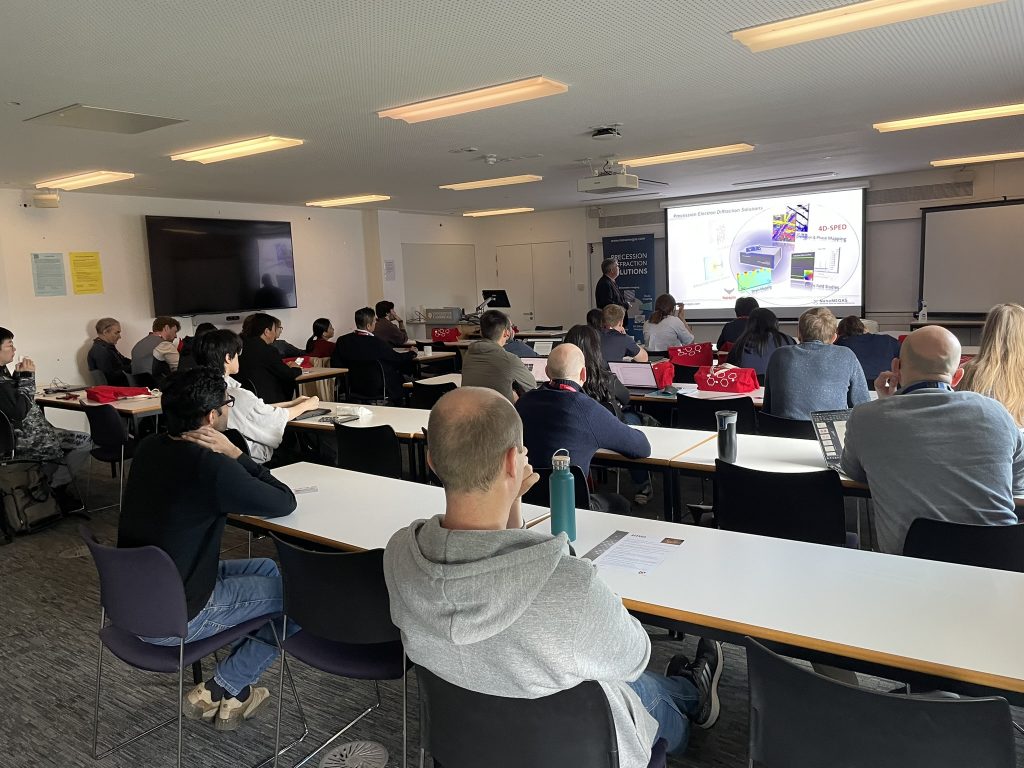
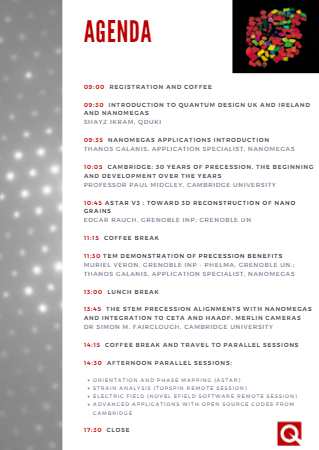
During the Workshop on the first day of the event, attendees heard from a number of speakers including:
- Dr. Shayz Ikram, Technical Director of QDUKI
- Thanos Galanis, Application Specialist of NanoMEGAS
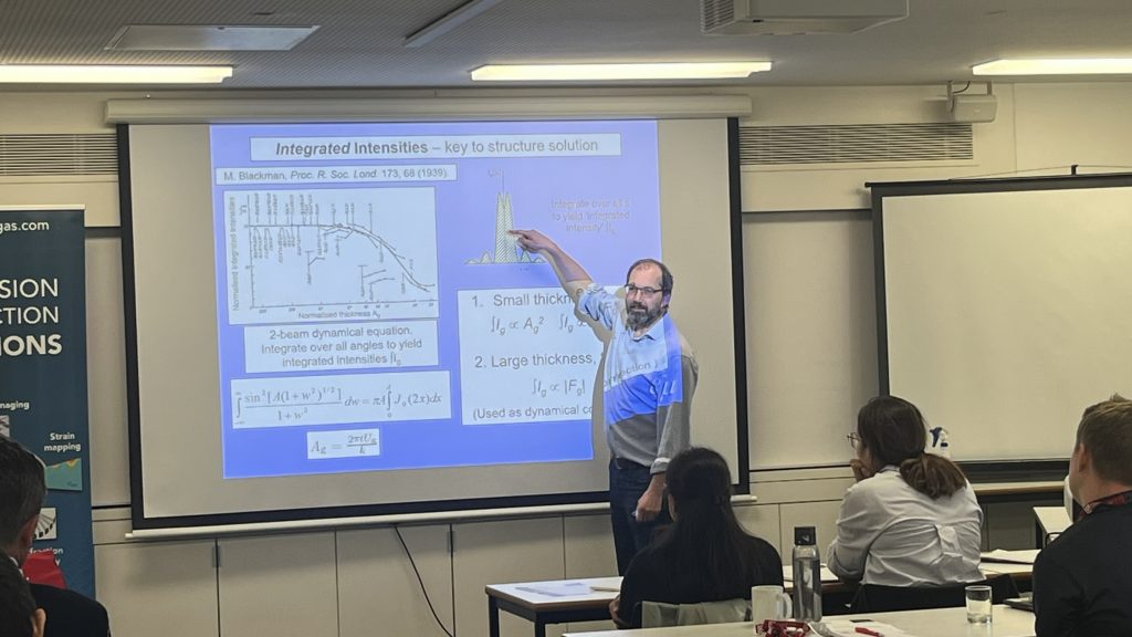
- Prof. Paul Midgley, Professor of Materials Science, University of Cambridge
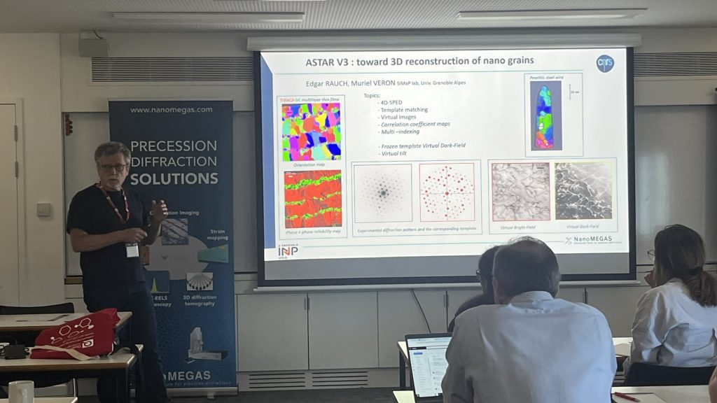
- Edgar Rauch, Grenoble Inp, Grenoble Un.
- Dr. Simon Fairclough, University of Cambridge
- Muriel Veron, Grenoble Inp – PHELMA, Grenoble Un.
In the afternoon, there were parallel sessions including:
- Orientation and Phase Mapping (AStar)
- Strain Analysis (TopSpin Remote Session)
- Electric Field (Novel EField Software Remote Session)
- Advanced Applications with Open Source Codes from Cambridge
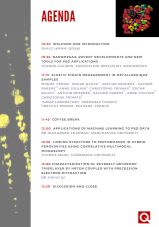
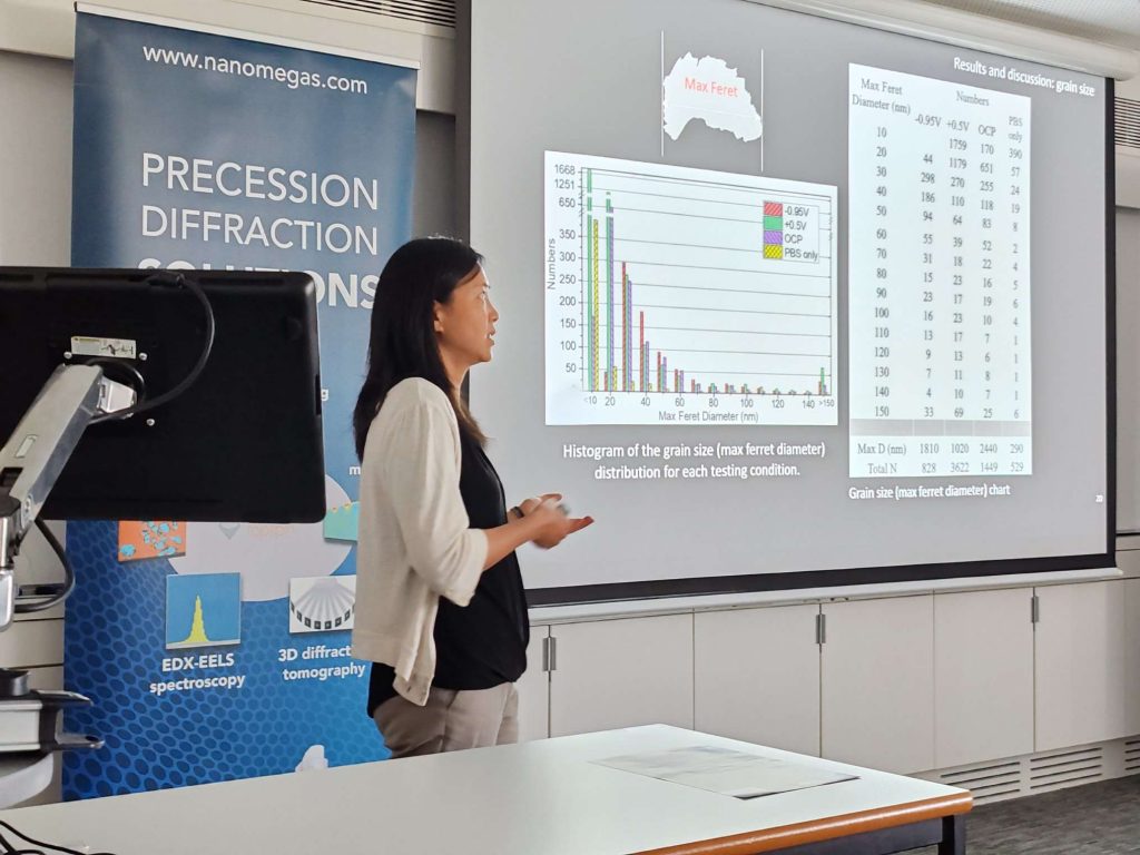
The following day was the User Meeting, where attendees were invited to hear about recent developments and new tools for PED applications and Elastic Strain Measurement in Metallurgique Samples. Dr. Alexander Eggeman of the University of Manchester joined us again (having been with us at the 2022 workshop) to talk about the Applications of Machine Learning to PED Data, then Thomas Selby from the University of Cambridge discussed Linking Structure to Performance in Hybrid Perovskites using Correlative Multimodal Microscopy.
“From novices to the most experienced, everyone was amazingly engaged in all that the workshop had to offer. You could see that participants resonated with the great benefits of Precession Electron Diffraction through the combination of lectures and practical session in coding and on the Microscopes in the Wolfson Electron Microscopy Suites. Not only did we show the basics of PED but also some of the cutting edge; from observing eFields to advance data processing. It was a pleasure to host the event and we hope to have everyone back soon to do more PED.”
Dr. Simon Fairclough, Advanced TEM Technical Officer, Electron Microscopy Group, University of Cambridge
Award Presentation
We presented Paul Midgley, Professor of Materials Science at the University of Cambridge, with an award for his many achievements with Precession Diffraction over the last 30 years…
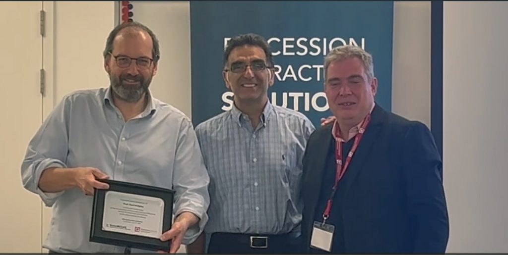
Professor Midgley’s interests lie primarily in transmission electron microscopy and in recent years he has focussed on the development of electron tomography, precession electron diffraction and energy loss spectroscopy and their application to nanoscale materials. Recently he has developed compressed sensing and machine learning algorithms tailored to the analysis of large multi-dimensional electron microscopy data sets.
He sits on the Editorial Boards of a number of journals and was for many years Editor-in-Chief of the journal Ultramicroscopy. He has received a number of awards and prizes including, in 2004, the Institute of Materials Rosenhain Medal and, in 2007, the Ernst-Ruska Prize of the German Microscopy Society. From 2008-2012, he was President of the European Microscopy Society and, from 2012-2016, the Past-President. In 2014 he was elected a Fellow of the Royal Society and, in 2016, an Honorary Fellow of the Royal Microscopical Society.
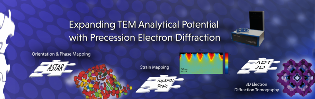
Phase Mapping
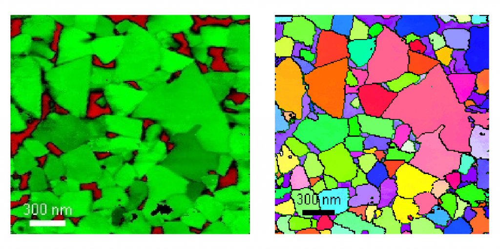
ASTAR device uses novel TEM based orientation/phase mapping technique to characterize any material down to 1 nm scale based on collection of precession electron diffraction patterns (PED). In combination with TOPSPIN acquisition of orientation / phase / strain/ STEM maps is possible
Strain Mapping
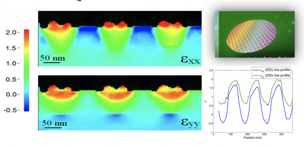
Novel Automated Strain Mapping Solution for TEM/STEM (Patent pending) based on nanobeam precession diffraction patterns and STEM reference image acquisition. Precision up to 0.02% (200kV FEG) with spatial resolution < 2 nm (FEG TEM). In combination with TOPSPIN acquisition of orientation /phase /strain /STEM maps is possible.
3D Diffraction Tomography
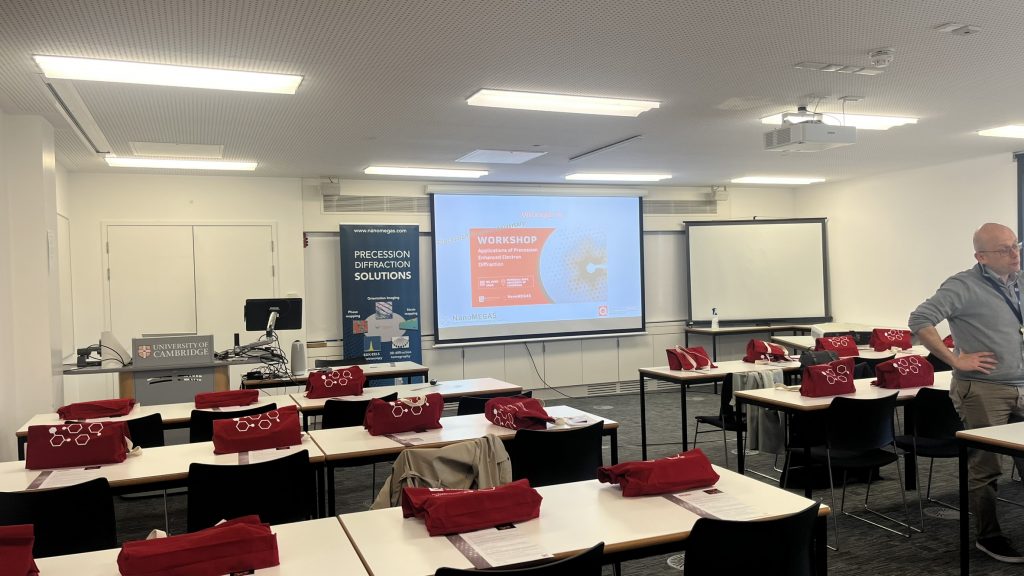
Workshop Agenda
User Meeting Agenda