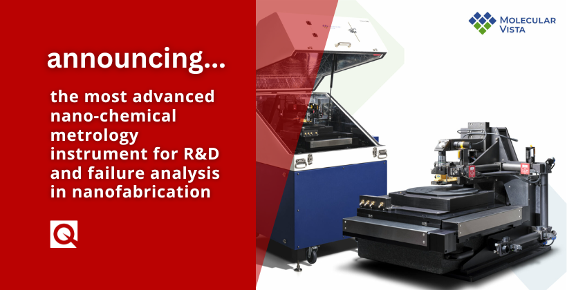
for R&D and failure analysis in nanofabrication
The Vista 300 from Molecular Vista is a nano IR instrument targeted for advanced semiconductor process monitoring and defect analysis.
Vista 300 combines an atomic force microscope with infrared spectroscopy to provide Photo-induced Force Microscopy (PiFM), a technique that performs chemical mapping with a spatial resolution of <5 nm, which is far superior to competing analytical methods like TOF-SIMS or XPS. PiFM provides chemical maps of compounds and molecular materials similar to how EDX performs elemental mapping at the nanoscale. While STEM-EDX has resolution similar to PiFM, it can only see atomic species. PiFM, however, maps and identifies molecules, be they organic or polymeric contaminants, inorganic particles or nanostructures, or EUV resist films and residues. PiFM is a noncontact technique, so samples remain clean, making PiFM ideal for analysing surface functionalisation (even down to monolayers) or identifying nanoscale defects and particles.
A remarkable demonstration of PiFM is shown in the accompanying images – PiFM is able to map the chemical differences between exposed and unexposed 16 nm half-pitch patterns in EUV resist before the resist is developed. AFM topography reveals no hint of the exposed pattern, but PiFM detects the chemical changes caused by EUV exposure.
Vista 300 is designed to handle full 300 mm wafers but does so in a minimal footprint of only 1.1 x 1.1 m2. The tool is fully developed and ready for immediate orders. Demonstrations of Vista 300 on customer wafers or other sample are available by contacting Dr. Shayz Ikram below.
In 2015, MVI was the first company to demonstrate <10nm resolution with nano IR (beating the competition by 10X at the time) and continues to lead the industry today with the introduction of new automation features that make PiFM easier than ever. MVI’s new AutoPiFM capability identifies materials and generates chemical maps and chemical fingerprint spectra with minimal user input required. Sit back and let AutoPiFM do the work! Likewise, MVI’s new AutoAlign system automatically and optimally focuses the IR optical beam on the AFM tip, eliminating the need for the user to learn the details of optical alignment. These features make PiFM fully accessible to laboratory or production technicians.
“With more advanced semiconductor processes dependent on atomically thin organic and dielectric layers with increasingly smaller feature sizes, Vista 300 is a perfect hybrid topography and chemical metrology tool for characterising High NA EUV lithography, selective atomic layer deposition, Cu-Cu hybrid bonding processes, and sub-100 nm defects.”
Dr. Sung Park, CEO of Molecular Vista


