


Combining AFM and SEM for the mechanical and electrical probing of nanostructures
In many research fields, there is a growing demand for in situ, multi-modal characterisation techniques that combine high-resolution imaging with real-time insights into electrical, thermal, and mechanical properties. Combining Atomic Force Microscopy (AFM), Scanning Electron Microscopy (SEM), and micromanipulators offers a synergistic approach to material characterisation and nanoscale analysis. Each technique provides unique capabilities, and their integration in one single setup enhances the scope and depth of the data obtained. This application note presents different examples highlighting the benefits of combining FusionScope and micromanipulators, such as mechanical and electrical analysis of individual nanowires, conductive AFM and Electrostatic Force Microscopy (EFM) of locally biased electrode structures, and characterisation of electronic devices.
Instrumentation
FusionScope is a highly versatile tool combining AFM, SEM, and Energy Dispersive X-ray Spectroscopy (EDS) capabilities into a highly integrated and easy-to-use workstation. It offers researchers a unique platform for easy sample positioning, data verification, and high-resolution surface analysis. Unlike other AFM solutions that employ a sample scanner design that limits the ability of simultaneously probing the sample during an AFM experiment, the FusionScope’s tip-scanning design for the AFM allows it to be easily combined with additional diagnostic measurement capabilities such as micromanipulators. In addition, FusionScope provides Profile View — an 80° tilt of the combined sample stage and AFM scan head. This enables precise positioning of the AFM tip, even on complex sample surfaces.
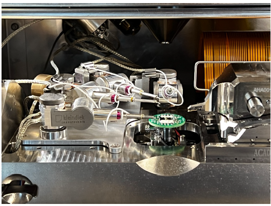
Kleindiek’s micromanipulators are well-established integrations in standard SEM or FIB systems. Due to their easy integration and excellent stability, they allow high-precision movement with sub-nanometer resolution. Their flexible design offers a broad range of applications ranging from mechanical manipulation to electrical probing, or electron beam induced current (EBIC) measurements. Up to four Kleindiek micromanipulators can be seamlessly integrated into the FusionScope system (see Figure 1) allowing for direct combination of AFM, SEM, and microprobing capabilities.
Mechanical and Electrical Probing of Individual Nanowires
Measuring the mechanical and electrical properties of individual nanowires is critically important because these properties determine how nanowires behave under various conditions, influencing their functionality and reliability in diverse applications. Electrical conductivity determines how efficiently the nanowires can transport charge, while understanding properties like carrier mobility ensures optimally designed high-speed low-power devices. In addition, mechanical strength, flexibility, and resilience affect the durability of the nanowire, especially in flexible electronics or wearable technologies.
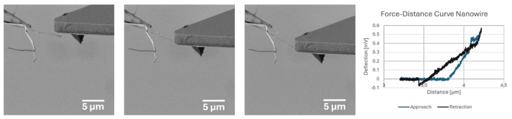
Workflow for Mechanical Probing of Nanowire:
The micromanipulator was used to pick up individual nanowires with a tungsten needle. This resulted in free-standing nanowires at the end of the micromanipulator tip. Using FusionScope’s Profile View, the nanowires could be precisely positioned below the AFM cantilever tip. The AFM then performed a force-distance measurement on the individual nanowire (see Figure 2). The complete force-distance measurement could be monitored simultaneously using the SEM. The collected data allows for the calculation of the mechanical properties of nanowire.
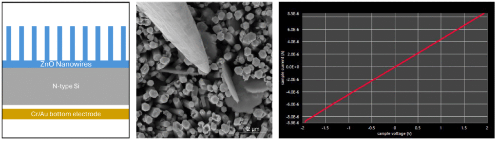
This example demonstrates the precise positioning and electrical probing capabilities of the FusionScope combined with Kleindieks’ micromanipulators. The sample used is an array of ZnO nanowires fabricated on top of a layer of N-type silicon substrate in combination with a Cr/Au bottom electrode (see Figure 3). The micromanipulator needle can be positioned on top of a single ZnO nanowire, and the electrical characteristics of the system are obtained by measuring the I/V-curve that shows an ohmic behaviour with a resistance of 230 kΩ.
Impact:
Understanding the mechanical and electrical properties of individual nanowires is fundamental in harnessing their potential in cutting edge technologies and ensuring their performance and reliability in practical applications. The combination of FusionScope and micromanipulators allows for easy characterisation of these properties by seamlessly combining all necessary measurement techniques in one single setup.
Combined Electrical Probing, Conductive AFM, and EFM of Electrode Structures
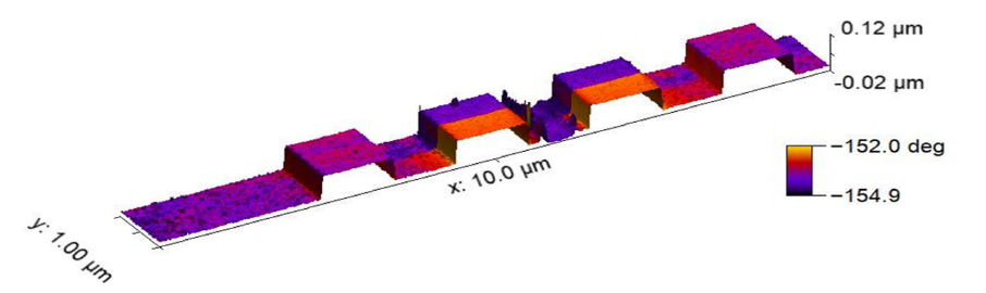
To demonstrate combined electrical probing and conductive AFM we used a sample containing eight independent electrodes on a silicon substrate, as well as an isolated gold electrode. The experimental setup involved selectively biasing individual electrodes using micromanipulators and simultaneously performing conductive AFM and EFM measurements.
Workflow for Combined Electrical Probing and Conductive AFM:
Two micromanipulators were positioned on the electrode structures using FusionScope’s Profile View. In addition, the conductive cantilever tip can be easily navigated in close proximity of the prober tips and positioned on the individual electrode structures. Simultaneous biasing of the electrodes and conductive AFM mapping can be performed (see Figure 4).
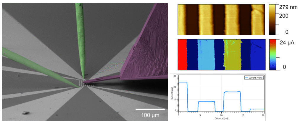
Workflow for Combined Electrical Probing and EFM:
Similar to the experiment above, two micromanipulators were positioned on the electrode structures.
This time EFM measurements were performed on top of the biased electrode structures. Only the
two inner most electrodes were biased. During the EFM measurement the applied bias voltage was
switched from +2 V to -2 V. As can be seen in Figure 5, the EFM signal shows a clear phase shift
due to the switching of the applied bias voltage.
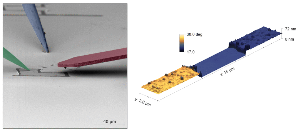
In a second example we created an isolated region on a silicon substrate coated with a 25 nm thin
gold film by using the Kleindiek micromanipulators to scratch part of the surface. This isolated gold
island was then biased with one of the micromanipulator needles to create a potential difference
between the island and the surrounding area (see Figure 6). A negative bias of -1 V was applied to
the gold island while the surrounding area remained grounded. An EFM measurement across the
border of the isolated gold island was performed to analyze the electrostatic characteristics of the
biased island and the surrounding grounded area. In the combined topography and overlayed EFM
phase-fly signal a clear contrast between the biased and the unbiased region can be measured.
Impact:
Combining electrical probing, conductive AFM, and EFM inside the FusionScope allows for detailed
electrical characterisation of different electrode structures. The ability to precisely navigate both
micromanipulator needles and the conductive AFM tip enables correlative analysis of electrical
devices under operation.
Benefits of Combining FusionScope and Kleindiek Micromanipulators
FusionScope’s multi-modal capabilities, combined with the precision of Kleindiek
micromanipulators, offer extensive new possibilities for nanoscale analysis and experimentation.
The ability to manipulate and electrically probe samples in situ while switching seamlessly between
AFM, SEM, and EDS allows for comprehensive new ways of surface characterisation.
- AFM provides ultra-high resolution for topographical, mechanical, and electrical properties.
- SEM provides fast overview scanning and easy location of the region of interest and positioning of micromanipulator needles and cantilever tip.
- EDS give detailed analysis of chemical composition of targeted area.
- Micromanipulators allow for localised electrical probing and mechanical manipulation.
The applications are manifold ranging from nanoscale device testing to in situ and real-time
characterisation in dynamic experiments. In summary, combining AFM, SEM, EDS, and electrical
probing creates a powerful synergy that integrates structural, topographical, and electrical insights
on the nanoscale.

Easy to use Correlative AFM with SEM Microscopy Platform
FusionScope is an easy-to-use correlative microscopy platform designed from the ground up to add the benefits of SEM imaging to a wide range of AFM measurement techniques.

Discuss Your Application Today
Get in touch with Dr. Luke Nicholls by email below or call (01372) 378822.


