- Features
- Specifications
- Videos
- Downloads
- Applications
- Related Products
- Back To Spectroscopy
- Back To Optics
- Back To Hyperspectral
- Back To Cameras
- Back To X-Ray
- Back To Light Measurement
- Back To Characterisation
- Back To Electron Microscopy
- Back To Magnetometry
- Back To Ellipsometers
- Back To Cryogenics
- Back To Lake Shore
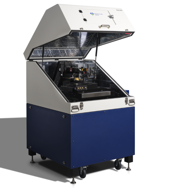
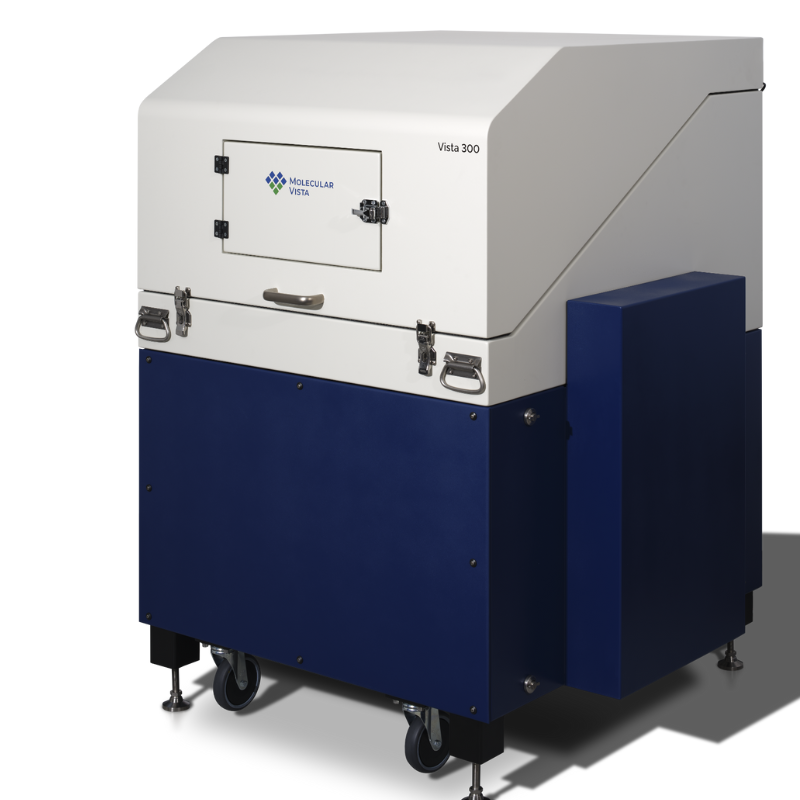
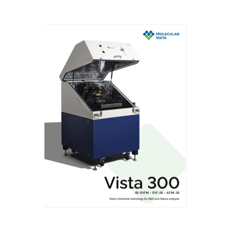
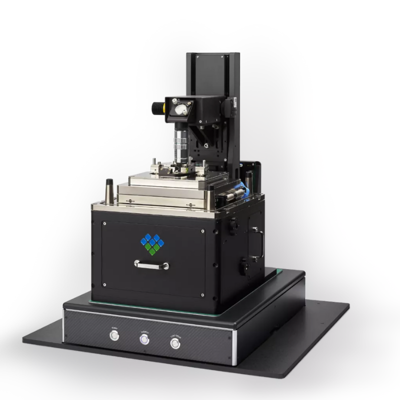
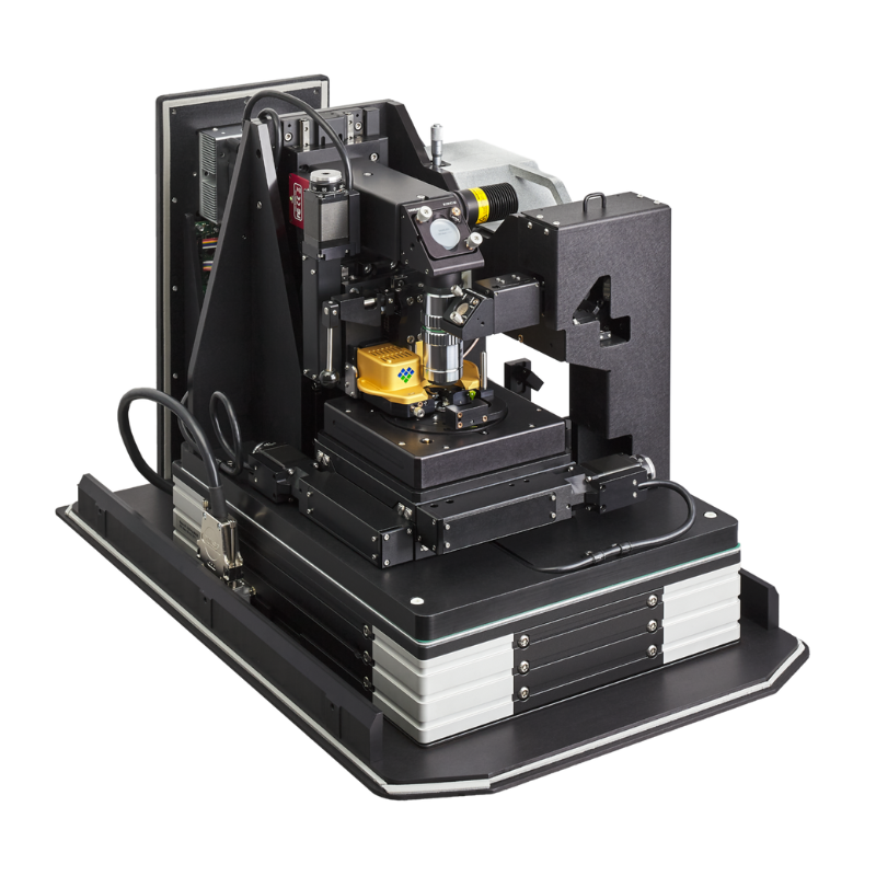
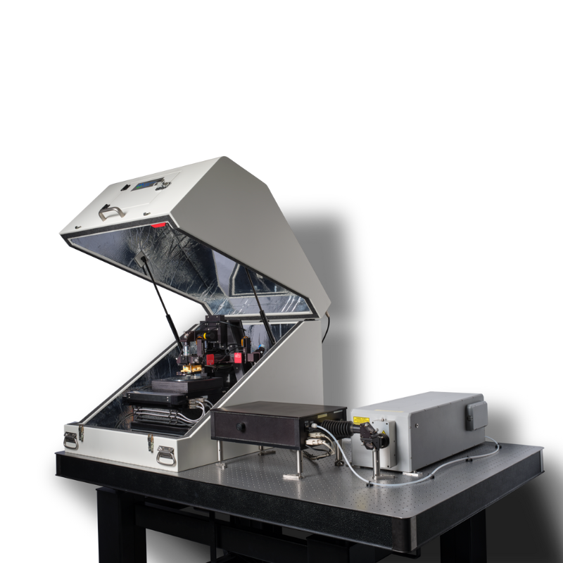
Molecular Vista “Vista 300” PiF microscope
Industry-leading automation
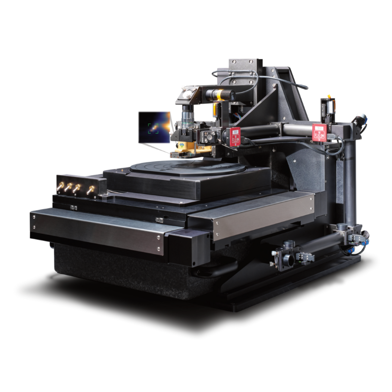
This instrument allows access to features on samples as large as 300 mm with PiFM & PiF-IR.
AutoPiFM and AutoAlign make Vista 300 the most advanced nano IR instrument ever made.
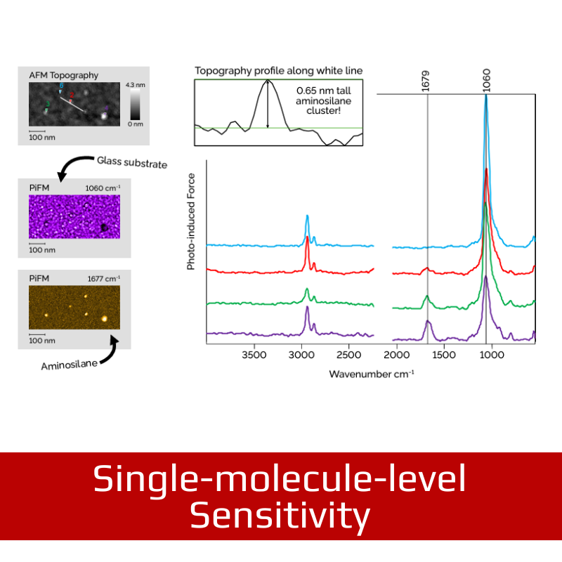
With sub-5 nm IR spatial resolution and single-molecule-level sensitivity, Vista 300 can help you efficiently solve tough problems in research, failure analysis, or fabrication facilities.
Vista 300 is the most advanced nano-chemical meteorology instrument for R&D and failure analysis in nanofabrication.
Features
AutoPiFM
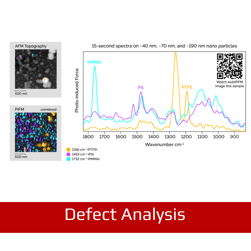
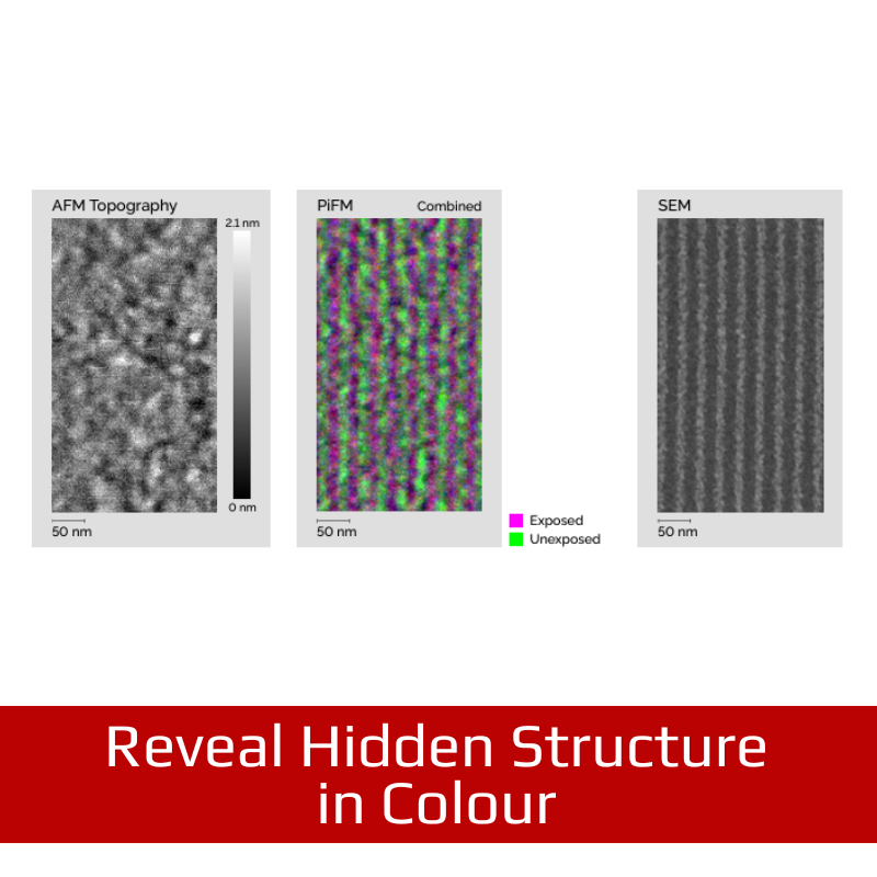
AutoPiFM generates a complete dataset from scratch, including fixed-wavenumber PiFM images of every chemical component detected, and PiF‑IR spectra in each chemical phase. Sit back and let AutoPiFM do the work!
Automatic alignment
An industry first! The critical alignment of the excitation laser is now performed using computer vision, ensuring optimal results, reducing training, and saving time.
Compact footprint
Because of our automated beam alignment and integrated multiplexer, we can package the lasers below the main instrument. This creates a more compact design without compromises. Vista 300 supports up to two lasers to cover the full IR spectral range (see specifications).
Controlled environment
Maximise efficiency, minimise disruption
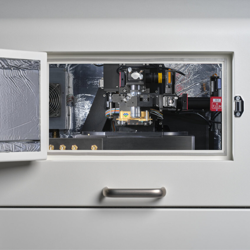
The 400 mm wide sample access door allows you to maximise throughput while minimising thermal disturbances that can cause drift. The insulated metal enclosure ensures acoustic isolation and stable temperature control within 0.1 °C, while also being clean room compatible.
Specifications
Stage and scanner
Sample stage travel: 300 mm × 300 mm square.
Scan size: 90 µm × 90 µm.
Dual Z Feedback: 12 µm z-scanner with 600 nm fast-z scanner provides both high bandwidth and a large z-range
Functionality
Imaging modes: Non-contact AFM, PiFM, KPFM, cAFM, nano DMA, FvD (force vs distance) mapping.
Spectroscopy modes: PiF-IR, FvD.
PiF Laser Options: QCL (770 – 1840, 1995 – 2395 cm−1), OPO/DFG (590 – 2050, 2250 – 4400, 5000 – 7000 cm−1).
Depth probed (IR): 20 nm in surface mode & greater than 100 nm in bulk mode.
Physical requirements
System dimensions: Approximately 1.1 m × 1.1 m × 4.9 m (3’ 7.3” × 3’ 7.3”× 5”)
Enclosure: 400 mm × 200 mm access door minimizes thermal drift. The enclosure is removable without disconnecting cables.


