- Features
- Videos
- Downloads
- Applications
- Related Products
- Contact
- Back To Spectroscopy
- Back To Optics
- Back To Hyperspectral
- Back To Cameras
- Back To X-Ray
- Back To Light Measurement
- Back To Characterisation
- Back To Electron Microscopy
- Back To Magnetometry
- Back To Ellipsometers
- Back To Cryogenics
- Back To Lake Shore
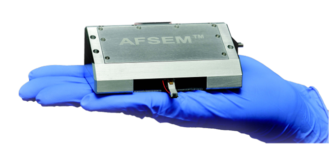
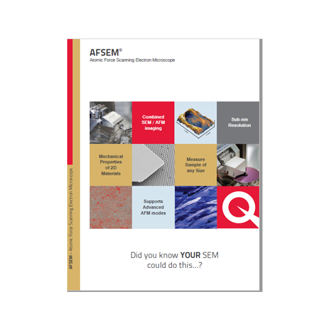
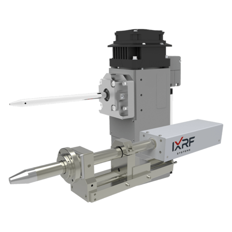
GETec AFSEM Atomic Force Scanning Electron Microscope
Combined SEM / AFM imaging
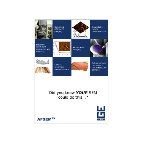
Did you know YOUR SEM could do this…?
AFSEM is an innovative instrument concept that combines the benefits of scanning electron microscopy (SEM) and atomic force microscopy (AFM) within one instrument. The AFSEM module is easily integrated into your existing SEM, and due to its unique design lets you use your standard SEM sample stage and other add-ons such as EDX or micro-indenter.
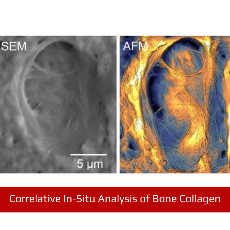
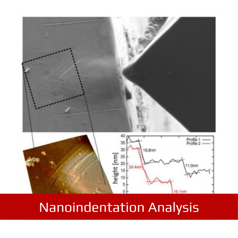
The complimentary capabilities of AFM and SEM allow for unique characterisation possibilities of your samples. AFSEM lets you image your sample with high resolution, create true 3D-topography representations and accurately measure heights, distances and even material properties, all while maintaining the large SEM field of view to position your AFSEM cantilever exactly where you want it.
Optimised workflow with practically no reduction of the SEM uptime enables you to reach seamless effectivity. The powerful control software allows for optimised measuring system handling and data analysis.
AFSEM fits into most SEM or dual beam (SEM/FIB) systems: it is mounted directly on the door of the system chamber, leaving the stage unaltered. In addition, a slim tip-scanning design in combination with self-sensing cantilevers requires only 4.5 mm space between the pole shoe of the electron column and the sample. As a result, AFSEM is compatible with a wide range of standard and optional stages, and can handle virtually any sample that fits the system chamber. This elegant design allows detection of sub-nanometer step heights in the SEM.
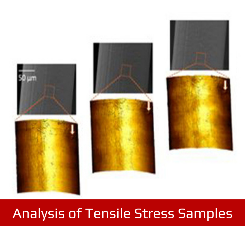
Due to its open access design, AFSEM is capable of imaging almost any sample size that your SEM can image. This is particularly useful when characterising semiconductor wafers, imaging large fracture surfaces for failure analysis, or when you need to hold your sample in custom sample holders. Because of its design, AFSEM is also compatible with many other add-ons that you may already have for your SEM, such as heating and cooling stages, mechanical stretching devices or mechanical manipulators. It can be removed from the SEM within minutes, and it can even be operated outside the SEM. The image quality has been given highest priority in the development of AFSEM, and state of the art AFM design concepts have been applied. The design has been optimised for linearity, accuracy and imaging speed using finite element analysis and model-based control algorithms. To optimise S/N ratio, the cantilever readout pre-amplifier has been integrated directly into the scanner unit. This has resulted in the AFSEM being capable of handling even challenging imaging tasks.
FEATURES:
- In situ AFM analysis in your SEM
- Correlative AFM and SEM analysis
- Compatible with most SEMs without impeding normal operation
- Many analysis techniques in parallel to AFM and SEM
- Intuitive handling with SCL’s self-sensing cantilever
Profile

Profile
Profile

Profile

Profile

Profile

Profile