In recent years there has been a huge interest in the nm scale characterisation of various materials (Minerals, Zeolites, MOFS, Aperiodic crystals, Archeological artefacts, Functional materials, Organic Pharmaceuticals, Proteins etc.).
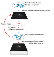
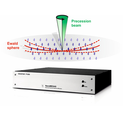
You will be shown the use of 3D Electron Diffraction (3D-ED) in the Transmission Electron Microscope (TEM) and present various examples demonstrating the application of the 3D-ED method to successfully solve structures. Using this method the crystal unit cell, space group, and atomic positions can be determined ab initio.
The study of nano-crystalline or amorphous materials can be optimally performed with Electron Pair Distribution Function (ePDF) in the TEM. This technique allows the study of materials at the local environment (nm scale) using collected (ED) patterns. We will show how ePDF has been recently applied to study nano-particles and amorphous materials.
The newly developed method of “4D-Scanning Nanostructure Electron Microscopy – nanostructure mapping” will be introduced. 4D-SNEM enables phase mapping of heterogeneous amorphous materials by collecting diffraction patterns from a region of interest and applying ePDF analysis to provide insight into structural variations at the local scale.