- Features
- Videos
- Downloads
- Applications
- Related Products
- Contact
- Back To Spectroscopy
- Back To Optics
- Back To Hyperspectral
- Back To Cameras
- Back To X-Ray
- Back To Light Measurement
- Back To Characterisation
- Back To Electron Microscopy
- Back To Magnetometry
- Back To Ellipsometers
- Back To Cryogenics
- Back To Lake Shore
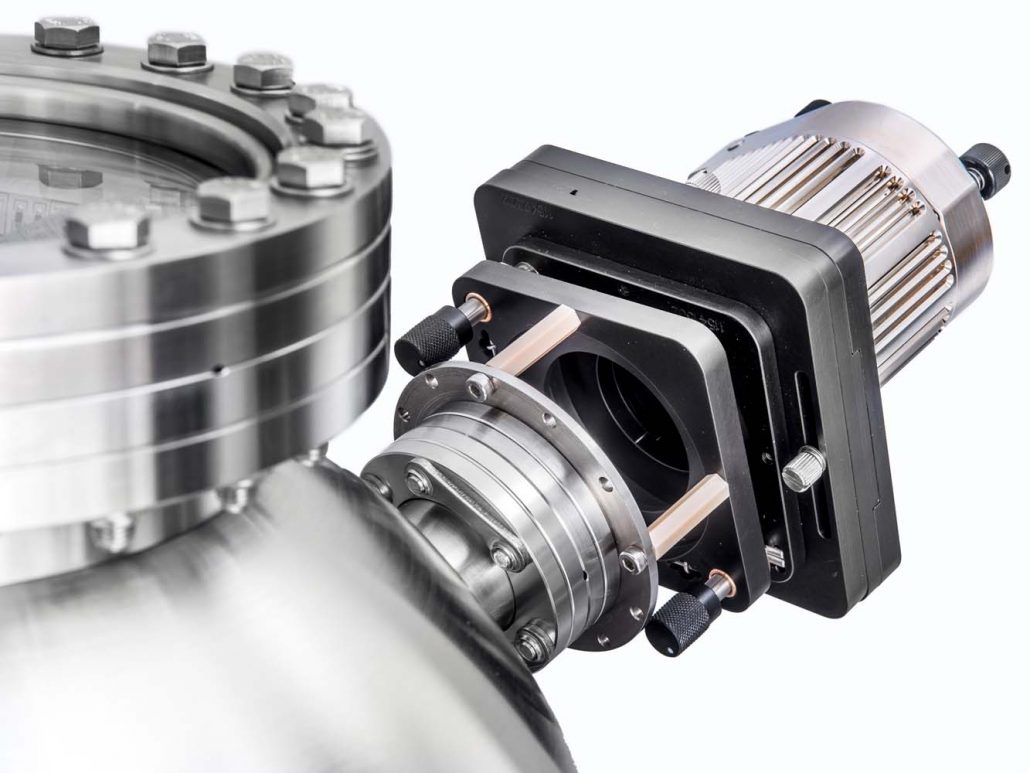
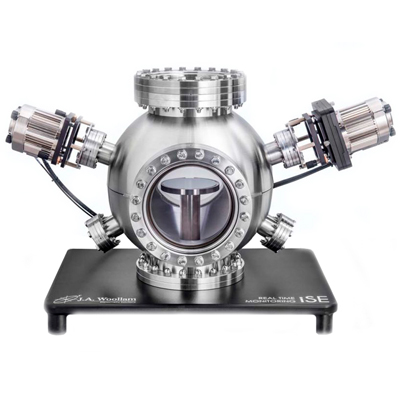
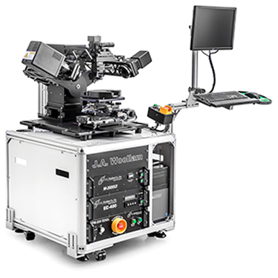
J. A. Woollam iSE Spectroscopic Ellipsometer
Ellipsometer for real-time monitoring of thin film processing
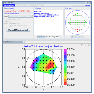
The iSE in-situ spectroscopic ellipsometer has been developed for real-time monitoring of thin film processing. Using Woollam’s proven technology, the iSE enables users to optimise optical properties of deposited films, control film growth with sub-angstrom sensitivity, and monitor growth kinetics, electric).
With the power of spectroscopic ellipsometry, the iSE is capable of measuring thickness and optical properties with much higher certainty than other techniques.
COMMON REAL-TIME ELLIPSOMETRY MEASUREMENTS
• Thin film thickness from single or multiple layers
• Growth or etch rates
• Process kinetics
• Optical constants
• Surface quality before and after processing
• Film nucleation behaviour
• Process conditions that affect optical constants (deposition rate, temperature, pressure, etc.)
• Real-time end-point detection
FEATURES
- Compact
- New compact design enables easy integration onto any ALD chamber
- Flexible
- Measure any kind of material-dielectrics, metals, metal oxides and more
- Affordable
- The power of spectroscopic ellipsometry at a reasonable price
- Ease-of-Use
- User friendly interface for real time data analysis and easy chamber integration
- Fast, Wide-Spectrum Measurements
- While others claim fast measurements, only J A Woollam ellipsometers provide fast, spectroscopic data over a wide wavelength range. The iSE utilises a new optical design with Dual-Rotation™ in combination with modern CCD detection to provide hundreds of wavelengths in a fraction of a second
VIDEOS
Downloads
Supplier Info
Applications
Photovoltaics
Film thickness and optical properties are critical to performance of solar devices. Ellipsometry is used for development and monitoring of all PV materials: a-Si, μc-Si, poly-Si, AR Coatings (SiNx, AlNx), TCO Films (ITO, ZnOx, doped SnO2, AZO), CdS, CdTe, CIGS, organic PV materials, and dye sensitised films.
Optical Constants
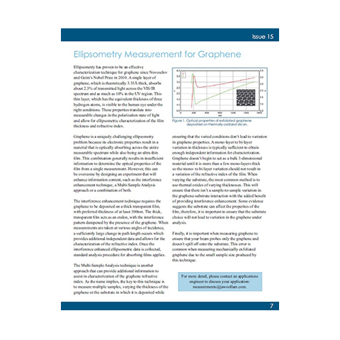
Thickness measurements are not independent of the optical constants. The film thickness affects the path length of light travelling through the film, but the index determines the light waves’ velocity and refracted angle. Thus, both contribute to the delay between surface reflection and light travelling through the film. Both n and k must be known or determined along with the thickness to get the correct results from an optical measurement.
Laser Optics
Accurate wavelength selection using monochromator allows measurements at the operating wavelength for optics, e.g. 1550nm, 1310nm, 980nm, 632.8nm, 589nm.
Thin Films
The film thickness is determined by interference between light reflecting from the surface and light travelling through the film. Depending on the relative phase of the rejoining light to the surface reflection, interference can be defined as constructive or destructive. The interference involves both amplitude and phase information.
Chemistry/Biology
The M-2000 can be used for a variety of chemical and biological applications, either as a stand-alone tool or in combination with one of our many accessories. Study materials under liquid ambient, at high or low temperatures, or in conjunction with QCM-D measurements.
Conductive Organics
Great progress has occurred in the area of organic layers and stacks used for display (OLED) or photovoltaic applications. There are many different materials being studied, from small molecules such as Alq3 to conjugated polymers such as P3HT. Often multiple materials are blended together – which requires the wide spectral range of the M-2000 – to probe different wavelengths where the organics are optically different. Long-chain molecules may also have significant anisotropy, where orientational stacking of the polymer chains produces different optical constants in different directions.
Semiconductors
Traditional ellipsometry applications are still going strong. Characterise any semiconductor material: resists, photomasks, SiON, ONO stacks, low-k dielectrics, high-k gates, SOI, SiGe, II-VI and III-V ternary and quaternary compounds.
Lithography
Lithography thin films were an important motivation for the VUV-VASE® development. It has been successfully used to characterise all types of films in this area, including Photoresists and Bottom and Top AR Coatings.
Metamaterials & the Meta-6 Layer
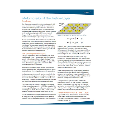
For ellipsometry, we usually consider only the electric-field component of the electromagnetic (EM) wave interaction with the material. We ignore the interaction of the magnetic-field component because atoms and molecules tend to have a weak magnetic response to EM waves at optical frequencies. Thus we usually consider only dielectric response (permittivity) and ignore magnetic permeability. However, certain kinds of metamaterials change all of that. Metamaterials consist of an artificially-created array of small structures or particles, usually smaller than the measurement wavelength. These structures or particles can be considered “artificial atoms” or “meta-atoms”, with properties tailored to interact with incoming EM waves in ways generally not observed in naturally occurring materials.