
Discover How to Scale Your Nanofabrication Capabilities
Venue: Royal Geographical Society in London
Date: 19-21 August 2026
Register here
Quantum Design UK and Ireland will be on Stand 19.
The UK has a solid international reputation as one of the leaders in Science and Technology, despite gaps in the technical workforce. The organisers believe nanoFabUK will contribute to closing this gap, giving the UK an edge over its competitors.
nanoFabUK’s vision is to connect nanofabrication RTPs across the country with the purpose of enhancing their expertise and stimulate innovation, through a range of knowledge exchange activities such as symposiums, technical workshops, and industry-led training events. The network will benefit not only RTPs who maintain this infrastructure, but also the academic and industrial end-users who rely on it through enhanced provision of nanofabrication services.
So How CAN you Scale Your Nanofabrication Capabilities?
Nanofabrication demands analytical tools capable of measuring, characterising, and validating structures at the nanoscale with exceptional precision. From thin-film deposition and semiconductor processing to advanced materials research, selecting the right instrumentation is critical for ensuring process control, material quality, and device performance. This guide explores some of the leading technologies used in nanofabrication, including spectroscopic ellipsometry, electron diffraction, correlative microscopy, X-ray microanalysis, and electron precession diffraction. Whether you’re working in a university cleanroom, industrial R&D facility, or advanced manufacturing environment, these solutions provide the insight needed to accelerate research and optimise fabrication workflows.

Quick FAQs, scroll down to read more about each solution…
The best ellipsometer depends on your application. The M-2000 Series is widely regarded as the industry standard for thin-film characterisation, while the RC2 offers maximum flexibility for advanced materials research. For in-situ process monitoring, the iSE is specifically designed for real-time measurements inside deposition and etch systems.
Spectroscopic ellipsometry provides non-destructive measurement of thin-film thickness, optical constants, composition, and uniformity. These parameters are essential for controlling deposition processes and verifying nanoscale device structures.
Electron diffraction enables atomic-scale structural analysis of nanocrystals and materials that are too small for traditional single-crystal X-ray diffraction. Systems such as the ELDICO ED-1 can analyse crystals as small as 10 nm while preserving beam-sensitive materials.
By combining SEM and AFM in a single platform, correlative microscopy allows researchers to rapidly locate, image, and characterise nanoscale features without transferring samples between instruments, improving efficiency and reducing contamination risks.
X-ray microanalysis is used to determine elemental composition, identify contaminants, analyse thin films, and support failure analysis. These capabilities are vital for validating fabrication processes and ensuring material quality.
PED is an advanced diffraction technique that improves the quality of electron diffraction data by reducing dynamical scattering effects. It enables highly accurate phase identification, crystallographic orientation mapping, strain analysis, and structural characterisation of nanomaterials.
Which is the Best Ellipsometer for Nanofabrication?
For nanofabrication, the best ellipsometers depend on your specific cleanroom needs, prioritising fast, multi-wavelength spectroscopy and the ability to measure small, patterned, or complex multilayer thin films…
1. M-2000 Series (Industry/R&D Standard)
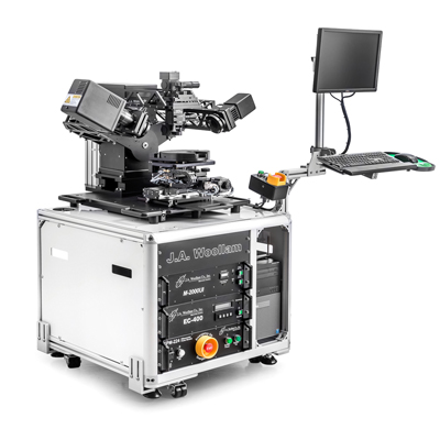
The M-2000 is the most popular spectroscopic ellipsometer in university and government nanofabrication facilities
- Key Features: Uses patented rotating compensator technology combined with high-speed CCD detectors to capture the entire spectrum (hundreds of wavelengths) in a fraction of a second.
- Best For: Fast, accurate thin-film characterisation. It handles a wide array of configurations, from multi-layer stacks to large-area uniformity mapping. It can be upgraded with focusing probes (beam down to ~100 µm) for small-area measurements
2. RC2 (Maximum Flexibility)
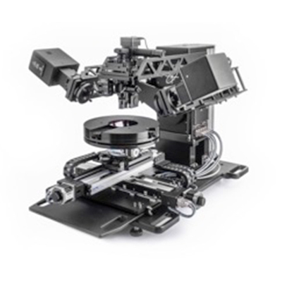
The RC2 is a highly advanced research-grade ellipsometer with a dual-rotating compensator design.
- Key Features: Captures the full Mueller matrix for highly complex samples, providing maximum accuracy and handling anisotropic (direction-dependent) or depolarising materials without special preparation.
- Best For: State-of-the-art nanofabrication labs working with novel 2D materials, quantum structures, and advanced optoelectronics.
3. iSE (In-Situ Monitoring)
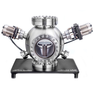
If you are doing fabrication inside a vacuum chamber, the iSE is engineered specifically for real-time monitoring
- Key Features: A compact design that can be mounted directly onto deposition or etch chambers to monitor film growth with sub-angstrom sensitivity in real-time.
- Best For: Process optimisation for Atomic Layer Deposition (ALD) or sputtering tools.
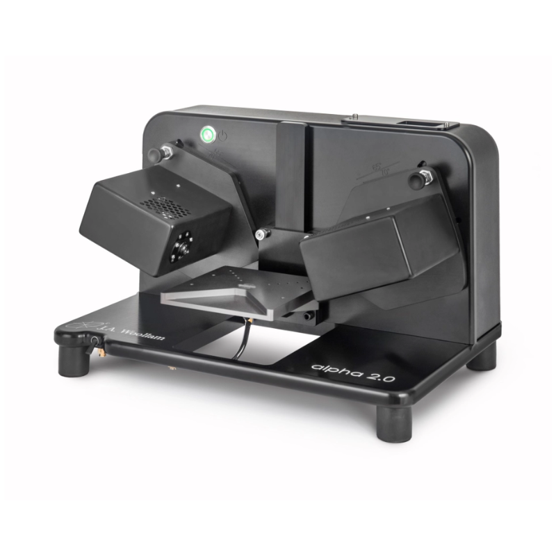
4. Alpha 2.0 (Routine Tabletop Use)
The Alpha 2.0 is an entry-level, budget-friendly tabletop system.
- Key Features: Great for rapid, routine measurements of single-layer dielectrics or basic multi-layer films. It has a smaller footprint and an easier learning curve.
- Best For: Smaller labs or quick daily characterisation where full-wafer mapping and advanced research features aren’t strictly needed.
5. VASE (Ultimate Wavelength Range)
The VASE is Woollam’s most established research system with the widest spectral range (from 193 nm in the deep UV to 33 \(\mu \)m in the far-IR).
- Key Features: Extreme flexibility in variable wavelength and variable angle of incidence (AOI).
- Best For: Nanophotonics and deep-UV lithography applications where highly specific optical constants (\(n, k\)) across a massive wavelength range are required.
Electron Diffractometer for Nanofabrication Applications

The ELDICO ED-1 is the world’s first dedicated electron diffractometer built specifically for nanocrystallography. It is ideal for nanofabrication and nano-analytics because it analyses particles as small as 10 nm and eliminates the need to grow large single crystals.
The ELDICO ED-1 enables fast, high-resolution atomic analysis of ultra-small structures through these key features:
- Disruptive Horizontal Design: Unlike traditional Transmission Electron Microscopes (TEM) repurposed for diffraction, its unique horizontal design features no lenses between the sample and the detector. This ensures fixed distances, superior geometric accuracy, and prevents the distortion of diffraction patterns.
- Nanoscale Structural Analysis: It effectively handles crystals in the 10 nm – 1,000 nm range, unlocking high-resolution datasets down to 0.84 Å.
- High-Precision 5-Axis Goniometer: Allows researchers to isolate and map phase mixtures, scan entire samples, and perform continuous rotations up to 140° while keeping the target crystal precisely in the beam.
- Beam-Sensitive Material Protection: Employs a low-dose STEM imaging mode and highly sensitive hybrid pixel detectors to capture atomic data quickly without destroying delicate nanostructures.
- Inert Transfer & Cryogenic Options: Protects reactive, unstable, or air-sensitive crystalline materials from oxygen and moisture to preserve their original state.
Correlative Microscopy for Nanofabrication
The Quantum Design FusionScope is a powerful correlative microscopy platform that physically combines Scanning Electron Microscopy (SEM) and Atomic Force Microscopy (AFM) into a single, seamless workflow.
By combining the high-resolution imaging capabilities of electron microscopy with the nanoscale measurement precision of atomic force microscopy, the FusionScope enables researchers to seamlessly acquire complementary structural, mechanical, electrical, and magnetic data from the exact same region of interest in real time.

Why Choose It?
Eliminates the “Needle in a Haystack” problem: Locating specific, nanoscale features (like nanowires or lithographically defined structures) using only a standard AFM takes hours of blind scanning. The SEM provides wide-field, high-resolution visual navigation, allowing you to instantly pinpoint a target.
Correlative 2D and 3D data: You can interactively overlay AFM 3D topography data onto 2D SEM images in real-time, giving you a complete, multi-dimensional view of your nanofabricated structures.

No sample transfer required: Because both microscopes are built on the same stage, you don’t need to break the vacuum or move your sample between separate machines, preventing contamination and saving immense time.
Benefits for Nanofabrication
Precise Probe Placement: The SEM column and AFM scan head can be tilted up to 80 degrees (Profile View), offering direct, real-time control to guide the AFM tip exactly to complex nanofabricated features
Electrical and Mechanical Characterisation: Using specialised cantilevers, it allows for Conductive AFM (C-AFM) and advanced modes like FIRE (Finite Impulse Response Excitation), letting you map electrical conductivity, IV properties, and surface stiffness of your fabricated devices.
Modular Upgrades: The chamber features extra ports, allowing you to easily add nano-manipulators, Backscatter Detectors (BSE), or Energy Dispersive X-Ray Spectroscopy (EDS/EDX) for direct elemental analysis of your materials.
Advanced Material Studies: It supports Magnetic Force Microscopy (MFM) to investigate magnetic domains, which is critical for nanoscale sensors and advanced data storage applications.
X-ray Microanalysis for Nanofabrication
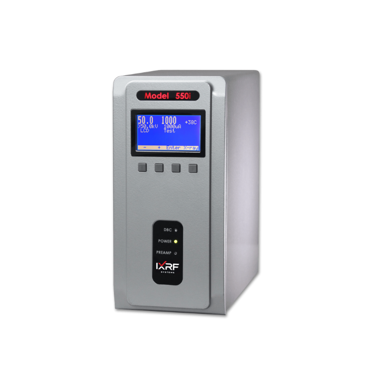
IXRF Systems specialises in high-end X-ray microanalysis solutions – specifically Energy Dispersive X-ray Spectroscopy (EDS/EDX) and micro-XRF – designed to be integrated with Scanning Electron Microscopes (SEM). While traditional nanofabrication relies heavily on lithography and deposition, IXRF provides the critical elemental mapping and failure analysis required to verify, troubleshoot, and validate nanoscale devices and materials.
Key Systems for Materials & Nanofabrication
- SEM/EDS Systems: IXRF engineers energy dispersive spectrometers that attach to SEMs and TEMs. These tools provide non-destructive elemental and chemical analysis at the micro- and nano-scale.
- SEM-XRF: IXRF pioneered SEM-XRF microscope attachments, which allow researchers to use both the electron beam and a micro-XRF beam simultaneously on the same sample. This provides excellent trace element detection—up to 10 to 1000 times more sensitive than standard SEM-EDS—making it highly effective for analysing thin films, semiconductor interfaces, and nanomaterials.
- ATLAS Apex Series: This is IXRF’s line of standalone, benchtop micro-XRF spectrometers. It features an industry-leading X-ray spot size down to 5 µm and uses multiple Silicon Drift Detectors (SDD) for rapid hyperspectral imaging of elements ranging from Carbon (C) through Uranium (U)
Applications in Nanoscale Research
Researchers use IXRF’s microanalysis equipment to:
- Analyse Thin Films: Verify film composition, uniformity, and thickness in semiconductor manufacturing and optical coatings.
- Characterise Nanomaterials: Evaluate 2D materials, nanoscale crystals, and nano-devices.
- Conduct Failure Analysis: Quickly identify contaminants or structural defects in fabricated micro/nano structures.

Electron Precession Diffraction for Nanofabrication
NanoMEGAS Electron Precession Diffraction (PED) is ideal for nanofabrication because it eliminates dynamical scattering effects (e.g., Kikuchi lines) from electron diffraction. By rotating a tilted electron beam around the central microscope axis, it generates “quasi-kinematical” (X-ray-like) data that enables precise, high-throughput structural analysis of nanostructures.
Key Advantages for Nanofabrication
Nanoscale Orientation and Phase Mapping (ASTAR)
- It maps crystallographic phases and orientations at an unprecedented 1 nm to 2 nm resolution. This allows manufacturers of semiconductors, nanowires, and battery materials to verify grain sizes, overlapping grains, and boundary thicknesses.
3D Diffraction Tomography
- PED allows the structural solution of unknown nanocrystals. By collecting a tilt series of 2D patterns, software reconstructs the reciprocal cell of any nanomaterial with a performance comparable to advanced synchrotron X-ray beamlines.
Strain Analysis
- The technology can be combined with software modules for ultra-precise strain mapping on multilayered nanostructures (such as semiconductors), ensuring structural integrity down to the nanometer scale.
Electromagnetic Field Mapping
- By tracking the center-of-mass (COM) displacement of the transmitted electron beam, 4D-SPED (Scanning Precession Electron Diffraction) can evaluate local electric or magnetic fields in active devices like sensors and transistors.
e-PDF (Pair Distribution Function)
- It delivers rapid structural profiling of amorphous materials and nanomaterials at the nanometer scale, outperforming standard X-ray PDF approaches by providing millisecond acquisition speeds.
Summary
Successful nanofabrication relies on a combination of advanced characterisation and analytical techniques. Spectroscopic ellipsometers such as the M-2000, RC2, iSE, Alpha 2.0, and VASE provide industry-leading thin-film measurement capabilities, while specialised systems like the ELDICO ED-1 deliver atomic-level structural analysis of nanoscale crystals. Correlative microscopy platforms such as the FusionScope streamline SEM and AFM workflows, IXRF microanalysis systems provide powerful elemental characterisation, and NanoMEGAS PED solutions enable detailed crystallographic and strain mapping. Together, these technologies help researchers and manufacturers improve process control, accelerate development, and gain deeper insight into the materials and devices that drive modern nanotechnology.
Contact Us
Want to understand the differences between the ED-1 and standard TEM-based electron diffraction? Or discuss specific applications relevant to your materials?
Get in touch with Dr. Shayz Ikram by email below or call (01372) 378822.