



Electrical characterisation at the nanoscale plays a central role in advancing semiconductor devices, nanomaterials, and next-generation electronics. However, probing individual nanostructures remains one of the more technically demanding aspects of modern microscopy.
Researchers carrying out electrical probing of nanostructures are increasingly looking for ways to bring imaging, probing, and surface analysis into a more unified workflow. The motivation is simple: reduce uncertainty, improve repeatability, and make it easier to connect electrical behaviour with physical structure.
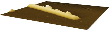
Why Electrical Probing of Nanostructures Is Challenging
Nanostructures are inherently difficult to access. Their small size and complex geometries make precise electrical probe placement extremely challenging. Even slight positioning errors can lead to missed contacts or unreliable data.
In traditional workflows, researchers rely on separate systems for imaging, electrical probing, and AFM analysis. This creates major inefficiencies:
- Slow and error-prone relocation between tools
- Increased risk of contamination during transfers
- Difficulty correlating electrical data with structural and surface properties
These limitations make nanoscale electrical characterisation both time-consuming and inconsistent.
How Correlative SEM-AFM Systems Improve Electrical Probing
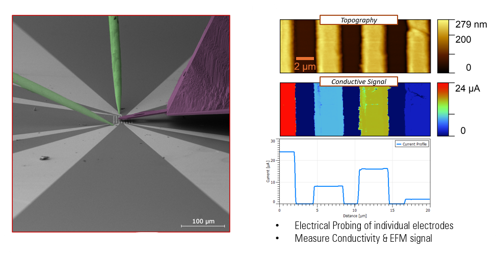
One way researchers are addressing these limitations is through correlative microscopy, where SEM and AFM capabilities are combined within a single environment. In an ideal SEM AFM combined system, imaging, probing, and measurement can happen without moving the sample between tools.
A shared coordinate system is a key part of this approach. It allows users to:
- Identify a region of interest (ROI) in SEM
- Return to the exact same location for probing or AFM
- Directly correlate structural, electrical, and surface data
This kind of integrated nanoprobing workflow reduces ambiguity between datasets and removes many of the inefficiencies associated with traditional multi-instrument setups.
Fast SEM-Based Positioning for Precise Electrical Probe Placement
Positioning probes accurately at the nanoscale is one of the biggest barriers to reliable measurements. SEM guided probe positioning helps address this by providing real-time, high-resolution imaging during probe approach.
With direct visual feedback, researchers can:
- Achieve faster and more reliable probe landing
- Reduce the likelihood of damaging delicate structures
- Improve the chances of forming stable electrical contacts
Compared to indirect or “blind” positioning methods, this significantly enhances nanoscale probe alignment and increases confidence in the resulting measurements.
Integrating Microprobers for Advanced Nanoprobing Workflows
Another challenge in nanoscale electrical testing is flexibility. Many experiments require more than a single contact point, especially when investigating device-like behaviour in nanostructures.
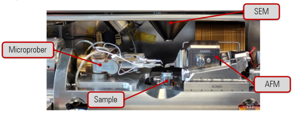
Workflows that support multiple microprobes open up additional possibilities, such as:
- Multi-point electrical measurements
- Device-level probing on nanoscale structures
- More adaptable experimental configurations
When microprobing is fully integrated into the same environment as imaging, researchers can perform complex experiments without repeatedly reconfiguring setups or relocating samples.
Combining Electrical Probing with AFM and EDS for Full Characterisation
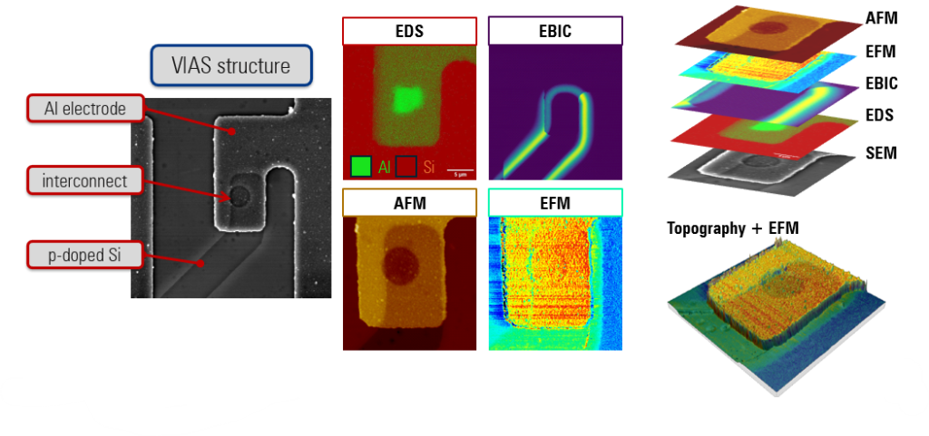
Electrical data alone rarely provides a complete picture. Understanding nanoscale behaviour often requires combining multiple complementary techniques.
An integrated approach allows researchers to correlate:
- Electrical probing → conductivity, current pathways
- AFM measurements → surface roughness, mechanical properties
- EDS analysis → chemical composition
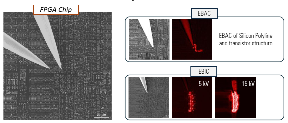
Additional methods such as Electron Beam Induced Current (EBIC) and Electron Beam Absorbed Current (EBAC) can further extend this capability, particularly in semiconductor failure analysis.
By linking these datasets directly, researchers can better understand how structure, composition, and surface properties influence electrical performance.
Targeted Electrical Characterisation of Nanostructures
Another common inefficiency in nanoscale workflows is the need to probe large areas without certainty about where meaningful signals will be found.
A more targeted approach allows users to:
- Screen large regions using SEM
- Identify specific nanostructures of interest
- Perform electrical measurements only where needed
This improves efficiency while increasing the likelihood that collected data is both relevant and reproducible.
Reducing Errors and Contamination in Nanoscale Workflows
Sample handling is a major source of error in nanoscale experiments. Each transfer between instruments introduces the risk of:
- Positioning errors
- Surface contamination
- Mechanical damage
Minimising or eliminating these transfers is central to achieving contamination-free nanoprobing. A more integrated nanotechnology workflow can significantly reduce these risks, leading to cleaner data and more reliable results.
Applications: From Semiconductor Devices to Advanced Nanomaterials
These evolving workflows are particularly valuable in areas where precision and correlation are critical, including:
- Semiconductor device testing and failure analysis
- Electrical characterisation of nanowires and thin films
- Research on advanced nanomaterials and quantum devices
- FPGA and microelectronics analysis using EBIC/EBAC
By combining imaging, electrical probing, and surface analysis, researchers can build a more complete understanding of nanoscale systems—something that remains difficult to achieve with fragmented approaches.
So what’s the answer?
How do we make electrical probing of nanostructures easier?
Across all of these challenges—probe placement, data correlation, contamination risk, and workflow inefficiencies—a common theme emerges: researchers need a way to see, measure, and understand the same nanoscale feature without compromise.
What if those capabilities didn’t have to be stitched together across multiple tools?
What if imaging, probing, and analysis could happen in one continuous, coordinated workflow?
This is the thinking behind the FusionScope® correlative AFM‑SEM platform—designed to bring together the core techniques discussed throughout this article into a single, aligned environment.

At its core, this approach is built around true correlative microscopy—linking SEM, AFM, and analytical techniques through a shared coordinate system so that measurements can be performed on the exact same region of interest without relocation.
What This Enables in Practice:
- Correlative SEM-AFM workflows in one environment
Seamlessly move between high-resolution SEM imaging and AFM measurement while staying on the same nanoscale feature - Shared coordinate system for precise relocation
Identify a structure once and return to it reliably for electrical probing or surface analysis—without guesswork - Integrated nanoprobing workflows
Combine SEM-guided positioning with electrical measurements to improve probe placement accuracy and data reliability - Multi-modal characterisation in a single experiment
Correlate electrical, structural, mechanical, and chemical data without transferring samples between systems - Reduced contamination and transfer errors
Keep samples in one controlled environment, minimising handling and preserving sensitive nanoscale features - Faster, more intuitive workflows
Reduce time spent aligning, relocating, and reconfiguring—allowing more focus on interpreting results rather than acquiring them - Advanced measurement capabilities
Access techniques such as conductive AFM, EDS, and correlative imaging to explore electrical behaviour in context
A More Integrated Way Forward
For many researchers, the question is no longer whether these capabilities are needed—but how to bring them together in a way that is practical, reliable, and scalable across different experiments.
If your work involves nanoscale electrical testing, semiconductor failure analysis, or nanodevice characterisation, it may be worth exploring how a more integrated approach could simplify your workflow and improve your data quality.
FAQ: Electrical Probing of Nanostructures
It is the process of measuring electrical properties—such as conductivity or current flow—at the nanoscale using precision probes.
SEM provides real-time imaging that allows precise positioning of probes onto tiny structures.
It ensures that the exact same location can be revisited across SEM, AFM, and probing steps without manual realignment.
They are techniques used to analyse electrical behaviour in materials, often for semiconductor failure analysis and device characterisation.
Yes, integrated systems can support up to four microprobers for complex electrical measurements in the FusionScope.
AFM adds surface and mechanical data, enabling correlation between electrical performance and physical structure.
Explore the FusionScope platform
Free Electronic Failure Analysis Magazine

Our EFA magazine takes you inside the challenges of analysing complex circuit failures in advanced interlayer structures and explain how ellipsometry is unlocking new perspectives in materials and interface evaluation. We also highlight techniques for identifying sub-20 nm defects and ultrathin residues—issues that can silently compromise semiconductor reliability. Beyond materials analysis, we examine how infrared imaging is enabling truly contactless electronic measurements, offering new insights during development and troubleshooting.
Intrigued?
We believe the best ideas often start with a simple exchange. If you’re working on exciting—or challenging—our scientifically trained team would be glad to discuss it with you informally and see where the conversation leads. For all things FusionScope, get in touch with Dr. Luke Nicholls by email below or call (01372) 378822.


