


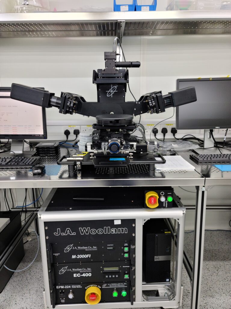
Woollam offers a range of spectroscopic ellipsometers (e.g. the M-2000 Ellipsometer, iSE Ellipsometer, etc.) that cover broad wavelength ranges (from the UV, through visible and IR) and support a variety of sample types — from dielectrics and semiconductors to metals, multilayers and complex stacks.
Because ellipsometry is non-destructive, non-contact, and extremely sensitive to very thin layers (even down to sub-nanometre changes), it is well-suited to analysing delicate or sensitive electronic structures without damaging them.
Woollam ellipsometers can support (or sometimes even enable) failure analysis in electronics, micro-electronics, semiconductors, coatings, or thin-film devices:
Thin film thickness and uniformity checks
In many electronic devices (semiconductors, passivation layers, dielectric coatings, oxide layers, barrier layers, interlayers) thin films are critical. Ellipsometry can measure their thickness and uniformity with very high precision. This helps detect deviations from design — e.g. layers being too thin, too thick, or non-uniform — which can cause failure (shorts, breakdown, leakage, insufficient insulation, etc.). Because ellipsometry is sensitive even at sub-nanometer scale, it can catch very subtle deviations.
Optical / material-property changes — indicating contamination, oxidation, degradation or damage
Ellipsometry can help deduce optical constants (refractive index, extinction coefficient, dielectric function), which correlate with material composition, density, crystallinity, presence of oxides or contamination, roughness, and more. If a layer has degraded (e.g. oxidised, aged, contaminated) or been physically/chemically altered, its optical properties will change — and ellipsometry can detect that non-destructively.
Multilayer / stack analysis in complex devices
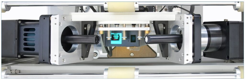
Modern electronics often use multilayer stacks — e.g. dielectric + metal + semiconductor + oxide layers, or complex passivation/insulation stacks. Ellipsometry can model and deconvolve such multilayers, giving insight into each layer’s thickness and optical behaviour.
That allows failure-analysis engineers to check whether an internal layer failed, degraded, delaminated, or otherwise changed.
Process-control, quality assurance, and detecting subtle manufacturing defects
Because ellipsometry can be fast and non-destructive, it can be used for routine inspection, QA, or failure screening — to catch defects early in manufacturing or after processing (e.g. after deposition, oxidation, etching, cleaning, or annealing). That helps avoid larger failures downstream. Woollam’s in-situ versions (like iSE) make it possible to monitor layer growth or etch processes in real time, potentially identifying problems as they arise.
Analysis of buried interfaces and detection of interfacial issues in semiconductor / thin-film devices
Ellipsometry (especially spectroscopic ellipsometry) can probe aspects such as optical constants and possibly electronic properties at or near interfaces — which can be critical when interface degradation, interdiffusion, or contamination leads to device failure. In research contexts, combining ellipsometry with other methods (e.g. photoemission) has been used to reconstruct band diagrams or examine interface quality in non-ideal heterointerfaces.
Why Woollam ellipsometers are especially useful in failure analysis
J. A. Woollam instruments stand out because:
- Broad spectral coverage — Their ellipsometers cover a wide range of wavelengths (from deep UV to IR), enabling analysis of a wide variety of materials and coatings (semiconductors, oxides, metals, organics, etc.). This flexibility is helpful when dealing with complex devices made from different materials.
- High sensitivity and precision — Ellipsometry from Woollam is sensitive enough to detect very thin films, subtle variations in optical properties, and small changes in surface or film conditions — critical for catching early signs of failure or degradation.
- Non-destructive and fast — Because it does not require destructive cross-sectioning or alteration of the sample (unlike e.g. cross-section SEM, TEM, or physical profilometry), it’s ideal for samples you need to preserve, validate, or return to customers/devices.
- Adaptability to multilayer stacks and complex structures — Modern electronics often use complex multi-layered films. Woollam ellipsometers are designed to handle such complexity, and sophisticated modelling (with their software) enables decomposition of multilayers to reveal thickness, refractive index, and more for each layer.
- Capability for in-situ or process monitoring — With dedicated systems (e.g. iSE), you can monitor deposition, etch, or other processing in real time — useful for quality control or diagnosing process-related failures before full device fabrication.
Typical Use Cases / Failure Scenarios Where Ellipsometry Helps
| Scenario | What ellipsometry reveals / helps diagnose |
| Thin-film passivation layer on a semiconductor degrades or becomes non-uniform, causing leakage | Detect changes in film thickness, roughness or refractive index — indicating thinning, oxidation or degradation. |
| Multilayer dielectric/metal/dielectric stack inside an integrated device shows degraded performance | Non-destructively inspect each layer’s thickness or optical constants to locate faulty or degraded one. |
| After a deposition or etch process, layer thickness is out of spec, risking device failure or poor yield | Non-destructively inspect each layer’s thickness or optical constants to locate faulty or degraded one. |
| Suspected contamination or oxidation at a buried interface affecting device reliability | Use spectroscopic ellipsometry (potentially complemented with other methods) to detect changes in optical constants or interface properties. |
| Quality assurance or failure screening for large batches of (sensitive) devices without destroying them | Rapid, non-destructive scans (thickness, uniformity) across many wafers or substrates to detect anomalies. |
Conclusion
Woollam ellipsometers provide a non-destructive, highly sensitive, and versatile optical metrology solution — making them a valuable asset in the toolkit for electronic failure analysis. By enabling precise thin-film measurements, multilayer stack analysis, in-situ process monitoring and material-property evaluation, they help engineers catch subtle defects, degradation, or process deviations that could lead to device failure.


