High-Tech Instrumentation for Electronic Analysis Failure
As device geometries shrink and architectures grow increasingly complex, understanding failure mechanisms has never been more critical. QDUKI offers cutting-edge methods that push the boundaries of what can be detected, measured, and understood.
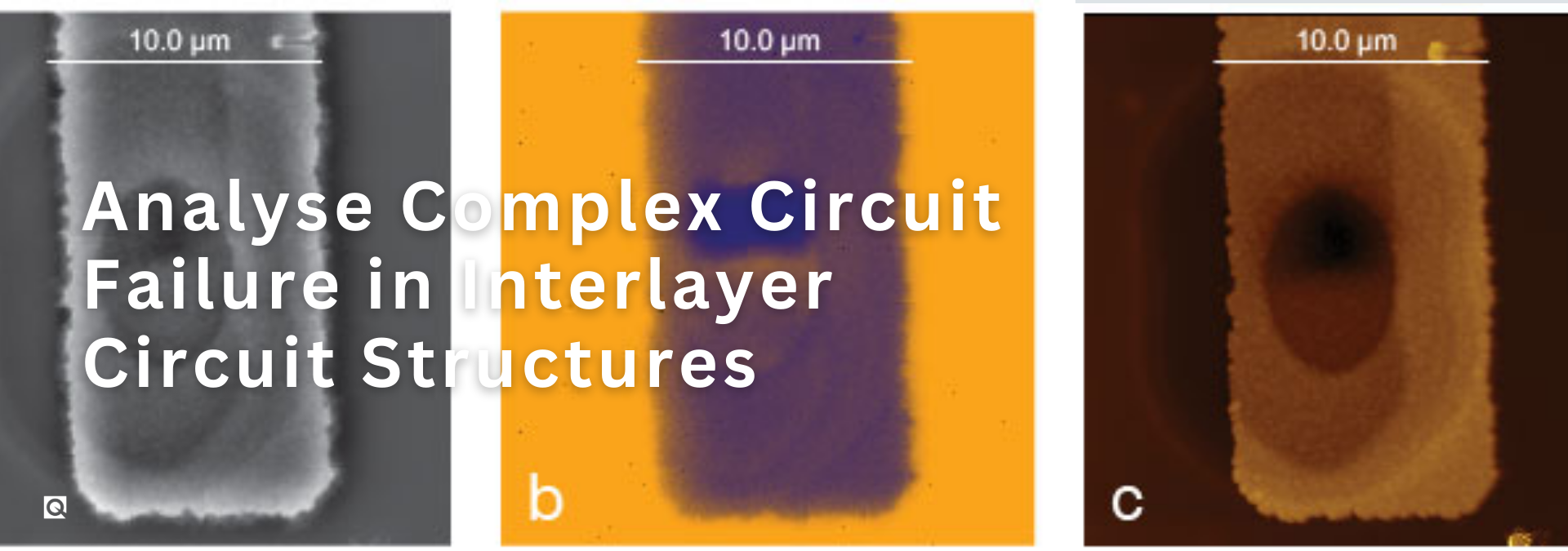
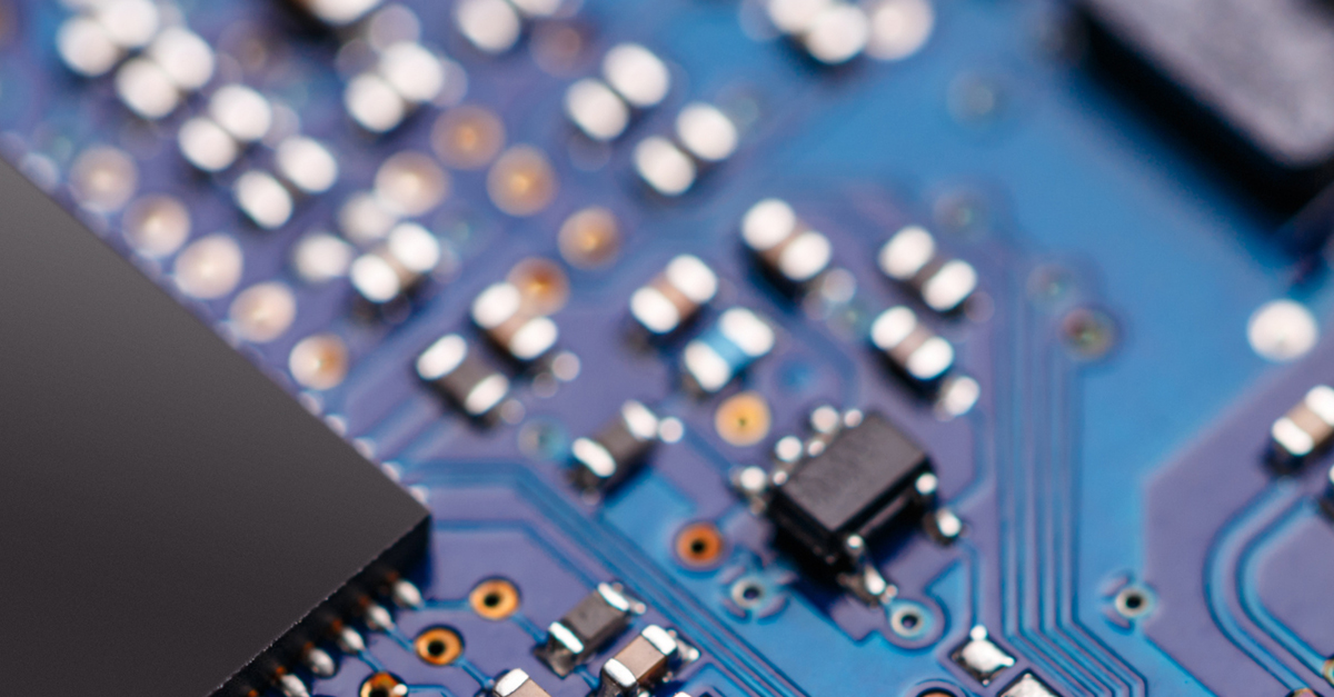
Our EFA magazine takes you inside the challenges of analysing complex circuit failures in advanced interlayer structures and explain how ellipsometry is unlocking new perspectives in materials and interface evaluation. We also highlight techniques for identifying sub-20 nm defects and ultrathin residues—issues that can silently compromise semiconductor reliability. Beyond materials analysis, we examine how infrared imaging is enabling truly contactless electronic measurements, offering new insights during development and troubleshooting.
Finally, a detailed case study shows how STMicroelectronics has successfully implemented the E-LIT solution across two sites.
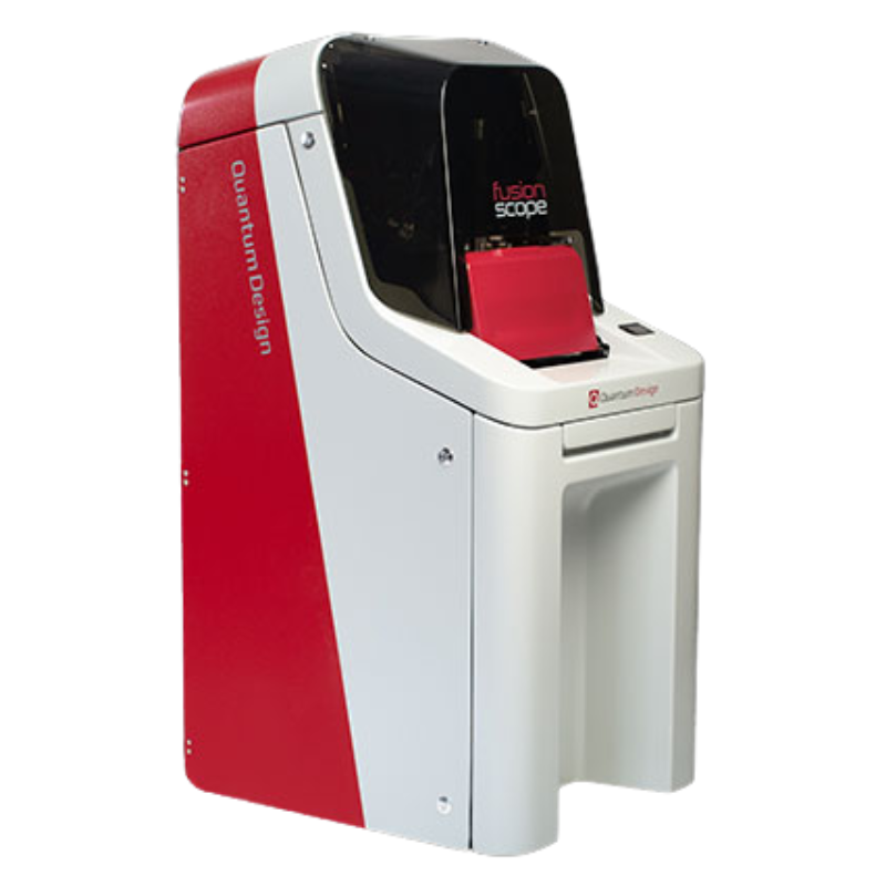
FusionScope Correlative AFM and SEM Microscopy
IXRF ATLAS M : micro XRF Spectrometer
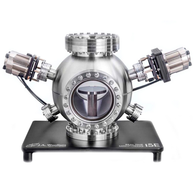
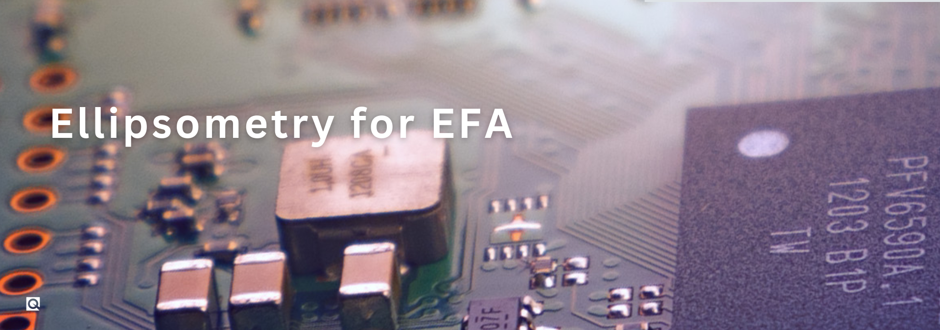
J.A. Woollam iSE Ellipsometer
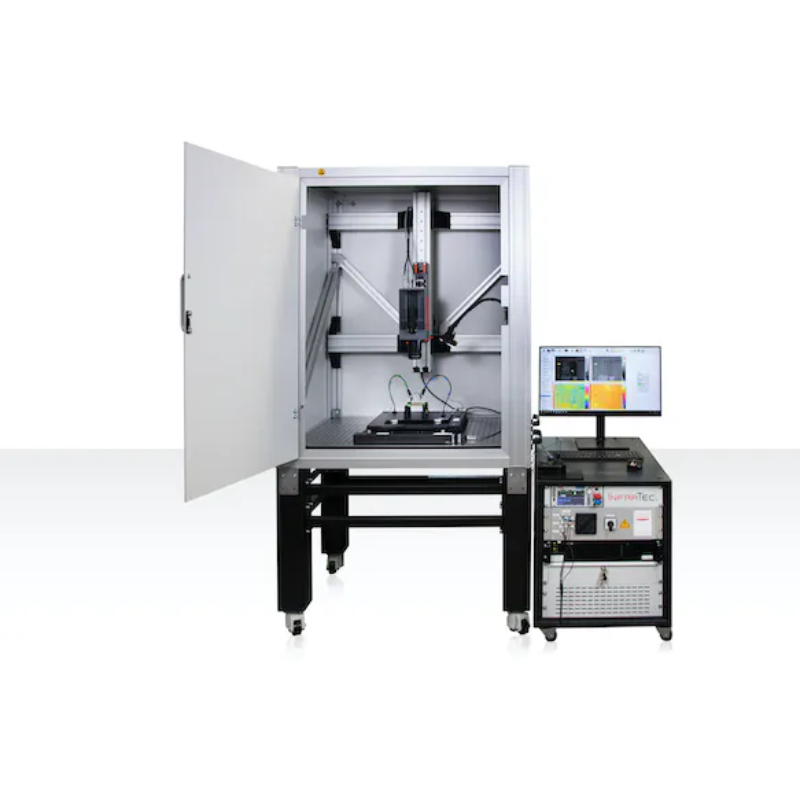
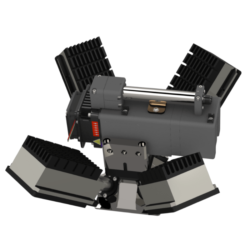
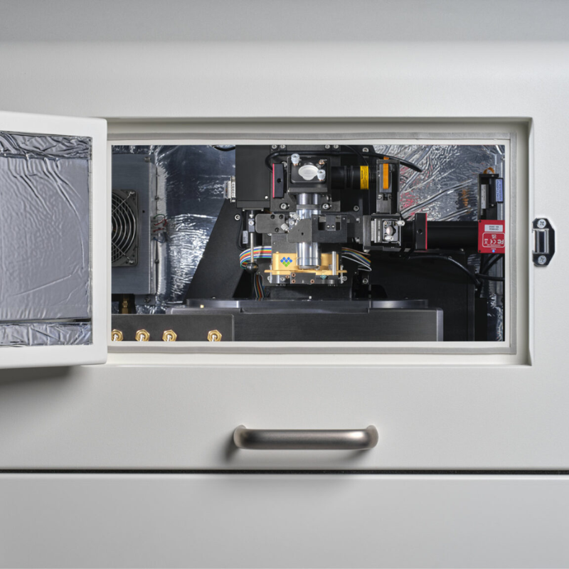
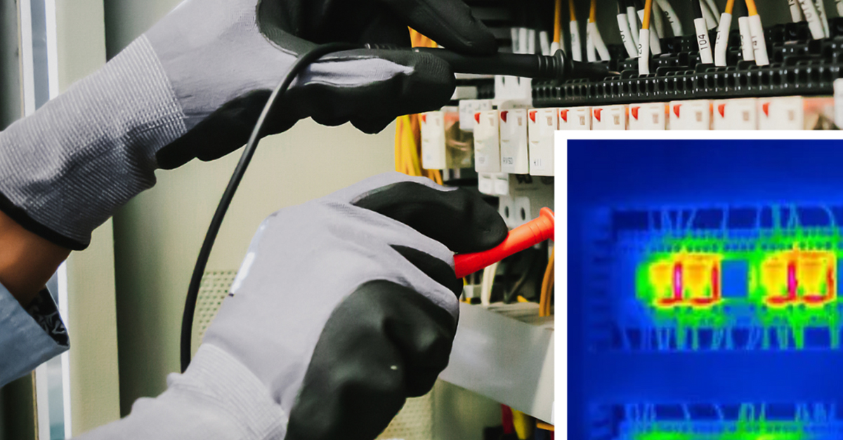
InfraTec Electronic / Semiconductor Testing Solution – E-LIT

Quantum Diamond Microscope
The Drive to Faster Data Transmission
With shrinking semiconductor device sizes and modern advanced packaging processes, it is crucial to eliminate sub-20 nm defects and surface contaminants.
While the presence of defects as small as 20 nm can be detected with survey tools, the traditional suite of analytical tools—such as XPS, ToF-SIMS, or SEM/TEM EDX—have difficulty in clearly identifying the contaminating source of defects, especially if they are organic.
Given PiFM’s sub-5 nm spatial resolution, even a multi-component defect can be de-composed into pure components via multivariate data analysis of PiF-IR spectra from different regions of a defect.
Molecular Vista Optical Microscopy Range
Fault Isolation on Chips and Power Modules
STMicroelectronics implements E-LIT solution in two plants
STMicroelectronics is a European manufacturer of semiconductor devices and integrated circuits with locations worldwide. Their products are mainly used in the automotive industry and for the Internet of Things (IoT). The company performs non-destructive failure analysis of chips, discrete components, sensors, LEDs and power modules using InfraTec’s E-LIT system in Shenzhen (China) and Calamba (Philippines).
The E-LIT solution employs lock-in thermography, a method, in which local defects are detected and analysed based on thermal anomalies generated by defined electrical excitation of an electronic component or assembly. At STMicroelectronics, the test system – comprising an excitation source, an infrared camera with adjustable Z-axis positioning and various lenses, an X-Y table, and additional accessories – was integrated into the failure analysis laboratory. The E-LIT system was further enhanced with a binocular to enable the connection of power supply contacts to the tested components.
ALL APPLICATIONS

Defence and Security

Aerospace

Quantum Science and Technology

Space and Astronomy
Semiconductors

Agriculture
Non-Destructive Testing